Polariton Panorama
D.N. Basov1, A. Asenjo-Garcia1, P.J. Schuck2, X.Y. Zhu3, Angel Rubio4,5
1.Department of Physics, Columbia University, New York, NY 10027, USA.
2.Department of Mechanical Engineering, Columbia University, New York, NY, USA
3.Department of Chemistry, Columbia University, New York, NY 10027, USA.
4.Max Planck Institute for the Structure and Dynamics of Matter, Luruper Chaussee 149, 22761 Hamburg, Germany
5.Center for Computational Quantum Physics (CCQ), Flatiron Institute, 162 Fifth Avenue, New York, New York 10010, USA
D.N. Basov, A. Asenjo-Garcia, P.J. Schuck, X.Y. Zhu, A. Rubio, Nanophotonics 10, 549 (2021)
Abstract: In this brief review, we summarize and elaborate on some of the nomenclature of polaritonic phenomena and systems as they appear in the literature on quantum materials and quantum optics. This summary includes at least sixty different types of polaritonic light-matter dressing effects unraveling a broad panorama of the physics and technology of polaritons. See also a recent review on Polaritonic Quantum Matter.
Polaritons are commonly described as light-matter hybrid quasiparticles. Polaritons inherit their attributes from both their light and matter constituents. More rigorously, a polariton is a quantum mechanical superposition of a photon with a matter excitation, the latter being a collective mode in solids and superconducting circuits or an electron in atoms, molecules or even superconducting qubits. As such, the notion of polaritons is a unifying universal concept between the fields of quantum materials and quantum optics/electrodynamics. Until fairly recently, these subfields of contemporary physics evolved largely independently of each other. Among the unintended consequences of these divisions is the ambiguity in polaritonic terminology with the same terms used markedly differently in quantum materials (QM) and cavity quantum electrodynamics (QED) in atomic systems. Here, we attempt to summarize (in alphabetical order) some of the polaritonic nomenclature in the two subfields. We hope this summary will help readers to navigate through the vast literature in both of these fields (Refs. 1–496). Apart from its utilitarian role, this summary presents a broad panorama of the physics and technology of polaritons transcending the specifics of particular polaritonic platforms (Cavity Quantum Electrodynamics and Cavity Polaritons –2). We invite readers to consult with reviews covering many important aspects of the physics of polaritons in quantum materials (D. N. Basov, Fogler, and García de Abajo 2016; D. N. Basov, Averitt, and Hsieh 2017; Low et al. 2017), atomic and molecular systems (Chang et al. 2018) and in circuit QED (Clerk et al. 2020; Carusotto et al. 2020), as well as general reviews of the closely related topic of strong light-matter interaction (Ruggenthaler et al. 2018; Forn-Díaz et al. 2019; McArdle et al. 2020; Frisk Kockum et al. 2019; Jestädt et al. 2019).
Cavity quantum electrodynamics and cavity polaritons
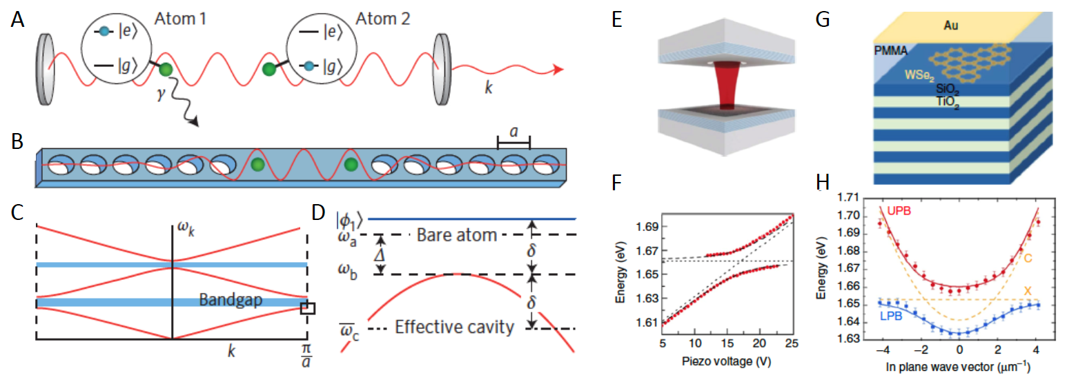
Cavity quantum electrodynamics and cavity polaritons. In cavity quantum electrodynamics (QED), the spontaneous emission of atoms, molecules and solids is governed not only by the properties of the emitter per se but is also controlled by its local electromagnetic environment. Optical cavities assembled from two parallel mirrors have long been used to confine light, to enhance light-matter interaction and to promote lasing (N. G. Basov 1965). The probability of interaction between light and matter is enhanced by the number of bounces the photon makes between the mirrors before leaving the cavity, which is conventionally quantified by the cavity finesse F. Cavities with high quality factors promote extremely efficient light matter couplings. In the strong-coupling regime (where the coherent interactions between the matter excitation and the cavity mode overcome the dissipation, i.e., when the vacuum Rabi splitting is much larger than the linewidth), the atomic or material excitation hybridizes with the photonic mode and produces a cavity polariton. The minimum separation upper polariton branch and lower polariton branch EUPB −ELPB in Panel H is commonly referred to the normal-mode splitting in analogy to the Rabi splitting of a single-atom cavity system (Deng, Haug, and Yamamoto 2010) (also Fig.4). Rabi splitting can reach fractions of eV in quantum materials and can exceed 1 eV in molecules (Schwartz et al. 2011; Stéphane Kéna-Cohen, Maier, and Bradley 2013). Strong coupling leads to photon blockade, where the presence of a photon in a cavity blocks a second one from coming in the study by Tian and Carmichael (Tian and Carmichael 1992) and Imamoğlu et al. (Imamoḡlu et al. 1997). See also microcavity polaritons.
Collective modes of a 2D superconductor
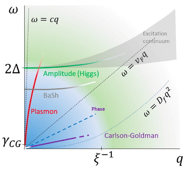
Figure 1: Schematic representation in the frequency–momentum plane of the collective modes that may appear in the electrodynamical response of a two-dimensional (2D) superconductor. The blue area shows the low-energy and long-wavelength region, where weakly damped collective modes may be observed. Anticrossing between the plasmon and Higgs mode and the Bardasis–Schrieffer (BaSh) mode is not shown here. Here, c is the speed of light, vF is the Fermi velocity, and Df is the normal-state diffusion coefficient. Adapted from a study by Sun et al. (Zhiyuan Sun et al. 2020).
Panorama of cavities and cavity modes
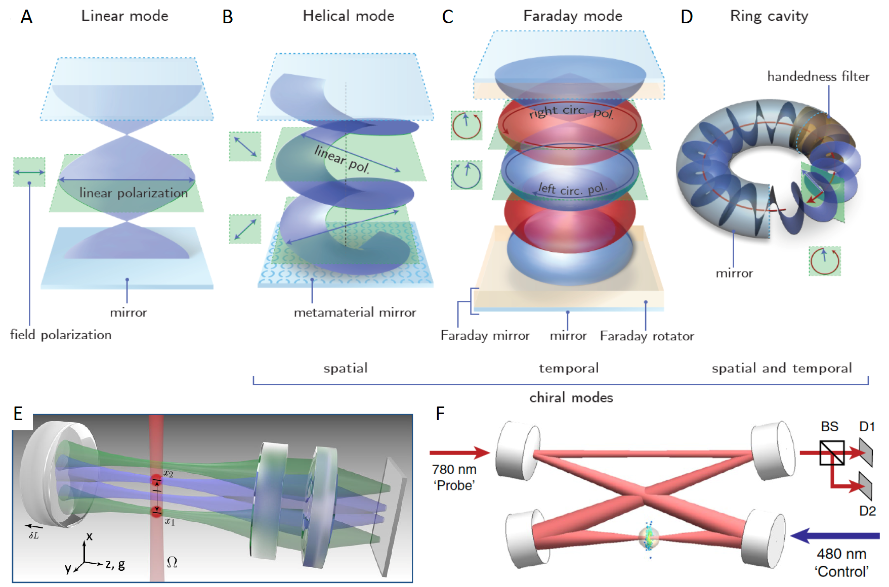
Box 2. Panorama of cavities and cavity modes. A common Fabry-Perot cavity (Panel A) formed by two parallel mirrors supports linear modes and maintains time-reversal symmetry. Cavities employing chiral meta-surfaces support helical modes (Panel B). A possible realization of time-reversal symmetry-breaking is offered by the use of Faraday mirrors in panel (Panel C). Ring mode cavities (Panel D) sustain running waves of a chosen circular polarization and break time reversal symmetry by means of a handedness filter realizable with a combination of a Faraday rotator and polarization optics. Advanced cavities are well suited for the exploration of the physics of spin vortices and skyrmion spin textures in exciton-polariton condensates originating from the optical spin Hall effect (Hübener et al. 2021; Vaidya et al. 2018). Panels A-D from Ref.(Jia et al. 2018). Panel E: multi-mode cavity QED enabling local light-matter coupling. The schematic displays two 87Rb Bose-Einstein condensates trapped at locations x1 and x2 on opposite sides of the cavity center (Faure et al. 2009). Panel F: schematic of a strongly interacting polaritonic quantum dot formed by 150 Rydberg-dressed Rubidium in a single-mode optical resonator (Donati et al. 2016). BS: beamsplitter; D1, D2: single-photon detectors.
Charged exciton-polaritons
Figure 2: Charged exciton-polaritons. Panels A: Two quantum wells, labeled with the indicies σ = 1, 2 and separated by a distance d, form an electron-hole bilayer in the extremely imbalanced limit. The minority species belongs to the σ = 2 layer, while the majority species at σ = 1 forms an interacting Fermi sea. Uq and Vq are, respectively, intra- and interspecies Coulomb interactions. The bilayer is located inside a planar cavity that confines the cavity photon mode C. The (blue) shaded area represents the finite-size external laser pump spot. Panel B: The same setup in a single quantum-well geometry. Here, the majority σ = 1 and minority σ = 2 species belong to the same well. Panels C and D: the particle-hole excitation process via a photon without and with) a Fermi sea, respectively. All photon-mediated transitions are approximately vertical in a cavity. Adapted from Ref (Tiene et al. 2020).
Interior and edge polaritons in van der Waals quantum materials
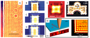
Figure 3: Interior and edge polaritons in van der Waals quantum materials. Panel A: charge transfer plasmon polaritons at the interface of graphene and a-RuCl3 visualized by means of nanoinfrared methods (ω= 898 cm−1 , T = 60 K). Three types of plasmonic fringes are observed: (i) edge plasmon polaritons (dark spots at along the physical boundary of graphene crystal), (ii) interior plasmon polaritons (oscillating wave pattern emanating from the boundary of graphene on the left), and (iii) defect-launched plasmon polaritons forming circular patterns in the interior of the sample. Adapted from a study by Rizzo et al. (Rizzo et al. 2020). Panels B– D: nano-IR imaging of edge plasmons on graphene nanoribbons. White dashed lines mark the boundaries of the crosscut GNR. Adapted from a study by Fei et al. (Z. Fei et al. 2015). Panel E: nanoinfrared image of edge plasmons in a square sample of graphene. Adapted from a study by Nikitin et al. (A. Y. Nikitin et al. 2016). Panels F: nanoinfrared images of edge phonon polaritons in the 25-nm-thick slab of hBN. Adapted from a study by Dai et al. (Siyuan Dai, Tymchenko, Yang, et al. 2018). Panel G: edge and interior phonon polaritons in a 40-nm-thick slab of hBN (P. Li et al. 2017).
Cavity Exciton Polaritons
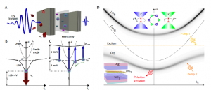
Figure 4: Cavity exciton polaritons. Panel A: polaritons (pink spheres with blue halo) emerge from strong coupling between the excitonic resonance in a quantum well (transparent sheet) and the photonic mode of a GaAs/AlGaAs microcavity. THz probing (blue curve) maps out the matter component of the polaritons, while photoluminesce (PL, red arrows) leaking through a Bragg mirror reveals the photonic component. Panel B: normal-mode splitting. The heavy hole 1s exciton resonance (dashed curve) and the photonic mode (dotted curve) are replaced by the upper polariton branch and lower polariton branch (UPB and LPB, respectively; solid curves). PL (thick red arrow) originates from the radiative decay of polaritons at small in-plane momenta k||. Panel C: THz absorption probes hydrogen-like intraexcitonic transitions. While the 1s state is spectrally shifted by strong light–matter coupling, the optically dark 2p exciton is not affected by the cavity. The resulting momentum dependence of the THz transition energy allows us to map out the momentum distribution of the polaritons as they relax toward k|| = 0 (green dotted arrow). From a study by Menard et al. (Ménard et al. 2014). Panel D: schematic of the valley ´ exciton polariton phenomena. The solid (gray) curves indicate LPB and UPB. The bare cavity and the exciton dispersion are shown by the black and orange dashed curves, respectively. Pump 1 is used to excite directly the exciton reservoir, whereas pump 2 excites the lower polariton branch at specific k|| and ω. The emission is collected at smaller angles. The top inset shows the valley polarization phenomena in 2D transition metal dichalcogenide (TMDC) semiconductors caused by the broken inversion symmetry. In these materials, the K and K′ points correspond to the band edges separated in momentum space but energetically degenerate. The bottom inset is a schematic of the microcavity structure with silver and a SiO2 cavity layer embedded with prototypical TMDC materials WS2. From a study by Sun et al. (Zheng Sun et al. 2017).
Phonon Polariton Figures
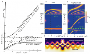
Figure 5: Phonon polaritons, hybrid plasmon–phonon polaritons, and image polaritons. Panel A: dispersion of phonon polaritons in ionic crystals predicted by Huang (in a study by Sun et al. (Zheng Sun et al. 2017). In the original publication, Huang did not use the term polariton. Panel B: calculated dispersion of the hyperbolic phonon polaritons in hBN (HP2). Panel C: calculated dispersion of the hyperbolic phonon polaritons in h-BN coupled to plasmon polaritons in the graphene layer and forming hyperbolic plasmon–phonon polaritons (HP3) and surface plasmon–phonon polaritons (SP3). Adapted from a study by Bezares et al. (Bezares et al. 2017). Panel D: concept of image polaritons at the interface of hBN and a metal. From a study by Yoo et al. (Yoo et al. 2021).
Moire Polariton Figures
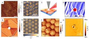
Figure 6. Moire polaritons and topological phonon polaritons in twisted van der Waals materials. Panel A: atomic force friction image of the graphene/hBN structure at the boundary between the moiré-superlattice and plain graphene (marked in Panel B). Moire reconstruction leads to a periodic pattern with the periodicity of 14 nm. Scale bar 1 mm. Panel B: nano-infrared image of the graphene/hBN structure. Darker contrast occurs in the moire region. The analysis of plasmon polariton fringes along the boundary between moire superlattice and plain graphene allows one to reconstruct the gross feature of the altered electronic structure in the moire superlattice region. Adapted from Ref. (Ni et al. 2015). Panel C: Nano-infrared image of plasmon polaritons interference patterns in a moiré superlattice formed by twisted layers of graphene. The dashed hexagons represent the boundaries of a single unit cell. From Ref. (Yankowitz et al. 2012). Panel D: Plasmon polariton superposition model, which accounts for the gross features of the image in C. Panel E: Schematic of the nano-IR imaging showing an AFM tip illuminated by a focused IR beam. Panel F: nano-infrared image of moire suprlattice pattern in hBN. The contrast is formed by the shift and broadening of the phonon polariton resonance. Adapted from Ref. (Yuan Cao et al. 2018). Panel G: nano-infrared image of phonon polaritons in a twisted structure of MoO3 slabs rotated by q =200, revealing complex wavefront geometry. Ref. (Kennes et al. 2020). Panel H: topological phonon polaritons in twisted MoO3 slabs rotated by q =770. From Ref. (Xian et al. 2019).
Ultra-fast plasmonic effects in van der Waals materials
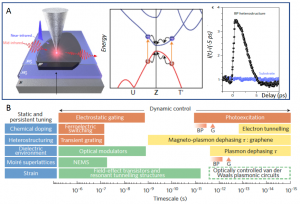
Ultra-fast plasmonic effects in van der Waals materials. Panel A: nano-infrared spectroscopy and imaging of switchable plasmon polaritons in black phosphorous (bP) semiconductor. Left: experimental schematics. Middle: Band structure of bP. Orange arrows indicate electron-hole pairs excited by a near-infrared pulse centered at a wavelength of 1,560 nm. The curved black arrows indicate carrier cooling towards the band extrema. Right: Ultrafast pump–probe dynamics of the scattered near-field intensity normalized to the signal at the negative delay time (equilibrium). The SiO2 substrate (blue points) shows no dynamics, whereas the SiO2/bP/SiO2 heterostructure (black points) features a strong pump–probe signal. Adapted from a study by Eisele et al. (Eisele et al. 2014). Panel B: Methods for controlling plasmons in van der Waals materials and the corresponding timescales. Static and persistent tuning methods are displayed in the blue boxes; dynamical control methods are displayed in the orange ones. The yellow boxes show the dephasing times (τ) of plasmons and magneto-plasmons in van der Waals materials along with characteristic timescales of electron tunnelling in these systems. The green boxes represent timescales pertinent for various photonics technologies. The box with the dashed green outline indicates the desired timescales for future ultrafast plasmonic circuits. NEMS: nanoelectromechanical systems; G: graphene. Adapted from a study by Basov et al. (Dmitri N. Basov and Fogler 2017).
Tip enhanced spectroscopy of plexcitons
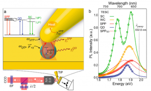 Figure 8: Tip-enhanced spectroscopy of plexcitons. Panel A: the strongly confined ∣Ez∣ field in a plasmonic nanogap cavity surrounding a single isolated CdSe/ZnS quantum dot (QD) and a tilted Au tip induce coupling between the plasmon and exciton. Panels B: Measured PL spectra for the QD, cavity plasmon polariton, weakly coupled system (WC) and strongly coupled states (SC) with coupling strength g = 141 meV. A Lorentzian lineshape representing the redshifted plasmon resonance in the presence of the QD is calculated from the fitted values (SPPQD) (May et al. 2020).
Infrared nano-imaging of polaritonic waves
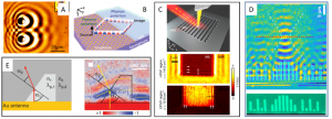 Figure 9: Infrared nanoimaging of polaritonic waves. Panel A: nano-IR image of the interference pattern of surface phonon polaritons on a SiC launched by circular Au discs (HUBER, OCELIC, and HILLENBRAND 2008). Panel B: prediction of inplane negative refraction between plasmon polaritons in graphene and phonon polaritons in an hBN slab (X. Lin et al. 2017). Panel C: nano-IR imaging of polariton evolution and canalization in an hBN metasurface (Peining Li et al. 2020). Panel D: optical images of the laser-written metalense (bottom). Nano-IR image of revealing focusing of phonon polaritons at 1452 cm−1 (Chaudhary, Tamagnone, Yin, et al. 2019). Panel E: refraction of graphene plasmon polaritons at the prism formed by bilayer graphene (P. Alonso-González et al. 2014).
Exciton Polaritons
Figure 10: Panel A: schematic of MoS2/WSe2 heterobilayer nanolaser integrated in photonic crystal cavity (Yuanda Liu et al. 2019). Panel B: polaron–polaritons in TMDC semiconductors. Schematic to illustrate the conduction and valence band structure and optical selection rules of monolayer MoSe2 close to the K and K′ points. An exciton in the K valley interacts with conduction band electron–hole pairs in the Fermi sea of the K′ valley to form an intervalley polaron. From a study by Bing Tan et al. (Tan et al. 2020) Panel C: experimental setup for the exploration of propagating solitons in the system of microcavity exciton polaritons (Sich et al. 2018).
Polariton waveguide QED
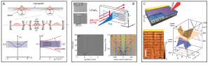
Figure 11. Polariton waveguide QED. Panel A: Emergence of bound atom-photon dressed states in 1D waveguides with finite bandwidth. The slow-light waveguide can be modeled as a large array of coupled optical resonators with nearest-neighbor coupling J. Lower left: band structure of the waveguide without atoms. Lower right: single-photon spectrum as a function of the atom-photon coupling g in the case of a single atom (with ωa = ωc) coupled to the waveguide, showing the emergence of bound states. Reproduced from a study by Calajo et al. (Calajó et al. 2016). Panel B: Photonic crystal for phonon-polaritons in LaTaO3. Top left: optical microscope images of the photonic crystal patterns. Top right: schematic of pump-probe experiments. Bottom left: Space–time plot of THz waves generated directly inside a square photonic crystal. The edges of the image are the edges of the photonic crystal. Bottom right: Dispersion diagram obtained from a 2D Fourier transform of the space–time plot in bottom left panel. The region highlighted in yellow represents the light cone. The regions highlighted in orange show the locations of the leaky modes.Adapted from a study by Ofori-Okai et al. [480](Ofori-Okai et al. 2014). Panel C: tunable and switchable photonic crystal for surface plasmon polaritons in graphene. Top: Schematic of a photonic crystal comprised of a graphene monolayer fully-encapsulated by hexagonal boron nitride on top of an array of SiO2 pillars. Pixelated gate insulator implemented in the form of nano-pillars enables the local modulation of the carrier density and therefore of the plasmonic density of states. Bottom left: near-field nano-IR image of plasmonic standing waves for a structure in the top panel. Scale bar 400 nm. Bottom right: Calculated plasmonic band structure as a function of wave-vector k and average carrier density ns. A vertical cut parallel to the ω-k plane (back panel) generates the plasmonic band structure at fixed carrier density ns=5.5×1012 cm2. The dashed lines mark the range of a complete plasmonic bandgap. A horizontal cut parallel to ns-k plane (bottom panel) generates the plasmonic dispersion as a function of average carrier density ns and wave-vector k, at laser frequency ω= 904 cm−1; a complete bandgap is evident for carrier density around ns=5.5×1012 cm2.
Anderson-Higgs polaritons
Bardasis-Schrieffer (BaSh) polaritons
Berreman polaritons
Berreman polaritons: Phonon polaritons in anisotropic materials and multilayer structures, also referred to as epsilon-near-zero or ENZ polaritons (X. Liu et al. 2015; Šik et al. 2000; Runnerstrom et al. 2017). ENZ materials, artificial structures and nano-cavities reveal exotic electromagnetic responses with a broad range of technological applications [27](Runnerstrom et al. 2017; Kelley et al. 2019; Alù et al. 2007; Javani and Stockman 2016; Thomas G. Folland et al. 2020). For example, ENZ nano-cavities facilitate ultra-strong coupling between plasmonic and phononic modes (Thomas G. Folland et al. 2020) as well as the so-called photonic doping (Liberal et al. 2017).
Berry plasmon polaritons
Berry plasmon polaritons: chiral plasmonic modes whose dispersion is explicitly impacted by the Berry curvature and anomalous velocity in chiral media (L. Shi and Song 2018; Kumar et al. 2016; Song and Rudner 2016). Berry plasmon polaritons are yet to be experimentally observed.
Bose-Hubbard polaritons
Bose-Hubbard polaritons: cavity QED polaritons with matter component associated with transitions across the Mott gap in the system of interacting atoms (Bhaseen et al. 2009) (see also Mott polaritons).
Bragg polaritons
Bragg polaritons. Bragg reflectors (Cavity Quantum Electrodynamics and Cavity Polaritons Panel G, Figs. 2 and 4) are routinely utilized to implement polaritonic cavities. Bragg polaritons pertain to systems in which multiple excitonic layers and/or quantum wells are periodically integrated in a DBR cavity (Faure et al. 2009; Goldberg et al. 2009) (see also polaritonic lattices). The inherent anisotropy of Bragg multilayer structures may enable hyperbolic electrodynamics(Sedov et al. 2015) (see hyperbolic polaritons).
Cavity polaritons
Cavity (micro-cavity) polaritons. Weisbuch et al. (C. Weisbuch et al. 1992) devised and implemented the first semiconductor (micro)cavity device revealing Rabi splitting of exciton polaritons (Cavity quantum electrodynamics and cavity polaritons and 2). Semiconductor microcavites emerged as a powerful platform for the investigation of strong light-matter interaction in semiconductors (Claude Weisbuch and Benisty 2005; Agranovich, Litinskaia, and Lidzey 2003). Microcavity structures reveal intriguing phenomena including the polariton parametric amplification (Savvidis et al. 2000) and its spontaneous counterpart, the parametric photoluminescence (Stevenson et al. 2000). Parametric photoluminescence is a purely quantum process. An appealing attribute of polariton parametric photoluminescence is that signal-idler polariton pairs are produced in non-classical states with quantum correlations. The quest for Bose-Einstein condensation of microcavity polaritons has produced a stream of breakthrough results (Deng et al. 2002; Guillet and Brimont 2016) (see also exciton-polaritons and their condensates). Microcavity exciton-polaritons display quantum effects including entanglement (Cuevas et al. 2018) and polariton blockade (Delteil et al. 2019; Muñoz-Matutano et al. 2019) and may serve as a platform for the implementation of qubits (Demirchyan et al. 2014).
Channel polaritons
Channel polaritons are supported by materials and structures with a straight channel cut in polaritonic medium (Novikov and Maradudin 2002). Channel polaritons were utilized for the implementation of waveguide components including interferometers and ring resonators (Bozhevolnyi et al. 2006). Polaritons guided along the nano-slit are predicted to form hybrid polaritons giving rise to both bonding and antibonding modes (Gonçalves et al. 2017).
Charge transfer polaritons
Charged polariton
Charged polariton. Charged polaritons posess a non-vanishing electric charge. This interesting concept was introduced in the context of the cavity exciton polaritons in GaAs/AlAs quantum wells that also hosted two-dimensional electron gas with the density ne. Spectroscopic experiments in (Rapaport et al. 2000) have identified several distinct properties of charged exciton polaritons, including the scaling of the coupling strength analogous to the properties of atomic QED system (Raimond and Haroche 1995). The effective mass of charged polaritons exceeds the band mass of a GaAs quantum well by a factor of 200. Tiene et al. have theoretically demonstrated the unique utility of charged micro-cavity polaritons for exploring the physics of electron-hole systems with charge imbalance, which are difficult to access with alternative experimental methods (Tiene et al. 2020). They demonstrated how the Fermi sea of excess charges modifies both the exciton properties and the dielectric constant of the cavity medium, which in turn affects the photon component of the many-body polariton ground state (Fig.2). See also the closely related entries of Fermi-edge exciton polaritons and trion polaritons.
Cherenkov polaritons
Cherenkov polaritons. In the Cherenkov effect (Cherenkov), a charged particle moving with a velocity faster than the phase velocity of light in the medium radiates light. The emitted radiation forms a cone with a half angle determined by the ratio of the two velocities. Genevet et al. demonstrated that by creating a running wave of polarization along a one-dimensional metallic nanostructure consisting of subwavelength-spaced rotated apertures that propagates faster than the surface plasmon polariton phase velocity, one can generate surface plasmon wakes that serve as a two-dimensional analogue of Cherenkov radiation (Genevet et al. 2015). The Cherenkov physics is also relevant to the properties of phonon polaritons (Auston et al. 1984; Maciel-Escudero et al. 2020). Infrared nano-imaging experiments reveal Cherenkov phonon polariton wakes emitted by superluminal one-dimensional plasmon polaritons in a silver nanowire on the surface of hexagonal boron nitride (Y. Zhang et al. 2020). See also Exciton-polariton X-waves on superluminal properties in the system of exciton-polaritons
Cooper pairs polaritons
Dark polaritons in QM
Dark polaritons in QMs: polaritons characterized by a wavevector that lies beyond the light line. The lower branches of polaritons in many/most QM systems are dark by this criterion and do not couple to free space photons because of the notorious “momentum mismatch” problem (Cavity quantum electrodynamics and cavity polaritons F, H, Fig.1).Light coupling to dark polaritons can be can be mediated by nanoscale defects such as a protrusions, divots, or cracks, exploiting the high spatial frequencies inherent to these deeply subwavelength objects. Better controlled strategies can also provide the missing momentum needed for coupling to dark polaritons (Barnes, Dereux, and Ebbesen 2003). These include prism and grating coupling, and the use of plasmonic optical nanoantennas (P. J. Schuck et al. 2005; Biagioni, Huang, and Hecht 2012; Novotny and van Hulst 2011; Baumberg et al. 2019; Tamagnone et al. 2018; Dubrovkin et al. 2020; Brown et al. 2018; X. Chen et al. 2019). Notably, sharp scan-probe tips can act as such antennas (Zhe Fei et al. 2011; P. James Schuck et al. 2013; Berweger et al. 2012; Park et al. 2018; B.-Y. Jiang et al. 2016; Keilmann and Hillenbrand 2004) allowing polaritonic waves to be launched and visualized. Scanning probe antenna-based nano-optics has emerged as an indespensible research tool enabling spectroscopy and visualization of polaritons in QMs (D. N. Basov, Fogler, and García de Abajo 2016; Brown et al. 2018; Atkin et al. 2012).
Dark-state polaritons in atomic ensembles
Dark-state polaritons in atomic ensembles: typically, this refers to polaritons in atomic ensembles that propagate in the regime of electromagnetically-induced transparency (EIT) (Fleischhauer, Imamoglu, and Marangos 2005; S. E. Harris, Field, and Imamoğlu 1990; Lukin 2003; Zoubi and Ritsch 2011). The darkness arises from the photon mixing strongly with a collective atomic excitation, resulting in a state with only a minute photonic component. See also EIT polaritons below. In ordered atomic arrays, dark (also often reffered to as subradiant) states emerge due to interference in photon emission and absorption. At the single photon level, these darks states are collective spin excitations with a wave-vector that lies beyond the light line, preventing the coupling with radiation modes (exactly the same phenomenon of “momentum mismatch” described above for QMs) (Bettles, Gardiner, and Adams 2016; Asenjo-Garcia, Moreno-Cardoner, et al. 2017; Shahmoon et al. 2017; Pines 1956). Polaritons arising in atomic lattices have applications in quantum information storage and processing (Shahmoon et al. 2017).
Demons
Demons: or density modes were introduced by David Pines (Pines 1956), an early protagonist of plasmons research. Demons are particularly relevant to the response of the Dirac fluid in graphene in hydrodynamic regime (Zhiyuan Sun, Basov, and Fogler 2018) and adiabatic plasmon amplification (Zhiyuan Sun, Basov, and Fogler 2016).
Dirac plasmon polaritons
Dirac plasmon polaritons are formed by hybrids of infrared photons with Dirac electrons in graphene (Jablan, Buljan, and Soljačić 2009; Woessner et al. 2015; Z. Fei et al. 2012; J. Chen et al. 2012). Direct nano-imaging experiments uncovered extraordinarily long propagation lengths of highly confined Dirac polaritons and have established fundamental limits underlying their decoherence and losses (Ni et al. 2018).
Dyakonov surface polaritons
Dyakonov surface polaritons: the surface modes that propagate along the interface between isotropic and uniaxial materials (D’yakono 1988; Takayama et al. 2009; Zubin Jacob and Narimanov 2008). A special case of Dyakonov polaritons is realized in anisotropic crystals of layered van der Waals materials. One example is that of the hyperbolic surface phonon polaritons propagating along the edges of slabs prepared from hexagonal boron nitride (Siyuan Dai, Tymchenko, Yang, et al. 2018; Alfaro-Mozaz et al. 2017; Dolado et al. 2020).
Edge magneto-plasmons
Edge magneto-plasmons. Two-dimensional (2D) electron gas subjected to the magnetic field normal to the plane of the 2D conductors reveals two distinct field-dependent resonances: the cyclotron resonance mode with frequency increasing with the magnetic field and another mode that redshifts with the applied field. The latter mode has been linked to the edge plasmons of the charged sheet and can be viewed as the 2D analog of surface plasmons in three dimensional (3D) systems (Mast, Dahm, and Fetter 1985). Specifically, edge magneto-plasmons can propagate along the physical boundary of the 2D conductors (Volkov and Mikhailov 1988; Kumada et al. 2014). Edge magneto-plasmons constitute a spectacular manifestation of the dynamical Hall effect. Edge magneto-plasmons are chiral. Their chirality is a direct implication of the applied Lorentz force (Petković, Williams, and Glattli 2014). Graphene reveals rich plasmonic phenomena in the presence of magnetic fields (Sadowski et al. 2006; Z. Jiang et al. 2007; Orlita et al. 2011; Z.-G. Chen et al. 2014; Nedoliuk et al. 2019).
Edge plasmon polaritons
Edge plasmon polaritons: one-dimensional plasmonic modes propagating along the physical boundaries of two-dimensional materials (Fig.3). Edge plasmon polaritons reveal an approximately 10 % shorter wavelength compared to the interior of the plasmonic medium (A. Y. Nikitin et al. 2016). Qualitatively, the shorter wavelength can be ascribed to the effective reduction of the Drude weight since free carriers exist only on one side of the physical boundary. Dyakonov hyperbolic phonon-polaritons are a lattice analog of edge plasmon polaritons. Berini reported on an in-depth numerical analysis of edge and corner plasmon-polariton modes in thin conducting slabs (Berini 2000).
Whispering-galley polaritons
Whispering-galley polaritons is a special example of an edge polaritons that loops around the ridge of polartonic medium (Lorente-Crespo et al. 2020) or along the cirumfrance of nano-holes (Rindzevicius et al. 2007; Degiron et al. 2004).
EIT in nanoplasmonic structures
EIT in nanoplasmonic structures (N. Liu et al. 2009; Taubert et al. 2012), EIT with plasmon polaritons in graphene (Yan et al. 2014; S. Xia et al. 2020) and EIT with exciton polaritons in microcavities (Walther, Johne, and Pohl 2018).
EIT polaritons propagate
EIT polaritons propagate in atomic systems under conditions of electromagnetically induced transparency (EIT). A remarkable aspect of EIT polaritons is that they can be slowed down to 10-s of meters per second (Hau et al. 1999) or even brought to a standstill (Kocharovskaya, Rostovtsev, and Scully 2001; Bajcsy, Zibrov, and Lukin 2003). EIT polaritons can be dark (decoupled from radiation, more “atom-like”) or bright (coupled to radiation, more “photon-like”). The darkness/brightness of the polaritons is controlled by an external laser beam. EIT polaritons can be strongly interacting, if coupled to Rydberg states (see Rydberg polaritons below). The EIT phenomenon is also observed in materials and nanostructures.
ENZ Polaritons
ENZ polaritons: epsilon near zero or ENZ polaritons are equivalent to Berreman polaritons above.
Exciton-polaritons and their condensates
Exciton-polaritons and their condensates. Exciton-polaritons are bosonic quasiparticles originating from photons hybridized with hydrogen-like bound electron-hole pairs. Semiconductor microcavities (Cavity quantum electrodynamics and cavity polaritons and Fig. 4A) offer an outstanding platform for the investigation of exciton polaritons and the attendant strong light-matter coupling. Provided a high-quality microcavity is nearly resonant with an excitonic transition, trapped photons may be emitted and reabsorbed multiple times before being lost to dissipation or cavity leakage. Absorption and re-emission of photons in the cavity gives rise to light-matter mixed eigenstates (C. Weisbuch et al. 1992). When sufficiently long-lived, exciton-polaritons may form coherent quantum states (Kasprzak et al. 2006; Carusotto and Ciuti 2013; Byrnes, Kim, and Yamamoto 2014). Bose Einstein condensates (BEC) of exciton polaritons are appealing quantum liquids in part because their coherent state is created and controlled by light (Griffin, Snoke, and Stringari 1995; High et al. 2012; D. Snoke 2002). The binding energies of excitons in organic molecules (Eisenstein and MacDonald 2004), transition metal dichalcogenides and lead halide perovskites can be as high as 0.75 eV (Deng, Haug, and Yamamoto 2010; D. W. Snoke and Keeling 2017; Y. Sun, Wen, et al. 2017; Lerario et al. 2017; Fu et al. 2019; Hanbicki et al. 2015; Cheiwchanchamnangij and Lambrecht 2012; Ramasubramaniam 2012; Komsa and Krasheninnikov 2012) these extraordinary high binding energies underlie the theoretical predictions of condensation and superfluidity at T=300 K (H. Min et al. 2008; Fogler, Butov, and Novoselov 2014; F.-C. Wu, Xue, and MacDonald 2015). BECs of exciton polaritons were predicted to form spatially and temporarily ordered states: time crystals (Nalitov et al. 2019). Exciton-polariton condensates may also enable energy-efficient lasers (Fraser, Höfling, and Yamamoto 2016).
Exciton-polariton X-waves
Exciton-polariton X-waves: wavepackets of exciton-polaritons that sustain their shape without spreading, even in the linear regime. In Ref. (Gianfrate et al. 2018). self-generation of an X-wave out of a Gaussian excitation spot is obtained via a weakly nonlinear asymmetric process with respect to two directions of the nonparabolic polariton dispersion. Notably, X-waves were found to propagate with superluminal peak speed with respect to the group velocity of the polaritonic system.
Fermi edge exciton polaritons
Fermi edge exciton polaritons (Gabbay et al. 2007; Pimenov et al. 2017) are observed in microcavities where the active semiconductor is heavily doped to form the Fermi edge. Fermi edge exciton polaritons are formed of electron hole pair excitations involving electron and hole states with in-plane wave vectors around the Fermi edge: kIIe=kIIh~kF where kF is the Fermi wavevector. In some litrature this latter form of polaritonic states are reffered to Mahan exciton polaritons (Baeten and Wouters 2015) recognizing a prediction of excitonic bound states in doped semiconductors beyond the critical density of the insulator to metal transition states by G. Mahan (Mahan 1967a; Mahan 1967b). See also Quantum Hall polaritons below.
Floquet polaritons
Floquet polaritons. The concept of Floquet engineering refers to the control of a system using a time-periodic optical field and is being broadly applied in atomic physics as well as in the field of quantum materials (Oka and Kitamura 2019). The notion of Floquet polaritons pertains to polaritons in a system of Floquet-engineered atomic states (Clark et al. 2019) or electronic states in solids (Mahmood et al. 2016). The concept of Floquet engineering by time-period optical fields has been extended to coherent phonons in quantum materials (Hübener, De Giovannini, and Rubio 2018). Chiral Floquet polaritons are predicted (Jia et al. 2018) to form in chiral cavities in which fundamental matter symmetries are broken (Box 2).
Frenkel exciton polaritons
Frenkel exciton polaritons. The matter constituent of these polaritons originates from Frenkel excitons characterized by the Bohr radii of the same order as the size of the unit cell. Frenkel exciton polaritons are common in organic semiconductors (Betzold et al. 2020). The high exciton binding energy (~eV) and large oscillator strength may lead to room temperature exciton-polariton condensates (Lidzey et al. 1998; Lerario et al. 2017; Keeling and Kéna-Cohen 2020).
Fuchs-Kliewer interface polaritons
Fuchs-Kliewer interface polaritons: phonon polaritons occurring at surfaces and interfaces (Foteinopoulou et al. 2019) with the matter part originating from Fuchs-Kliewer surface phonons (Kliewer and Fuchs 1966). Huber et al. (A. Huber et al. 2005) employed nano-infrared methods to visualize propagating Fuchs-Kliewer surface phonon polaritons in SiC. Surface phonon polaritons are observed in insulating and semiconducting materials including hBN (Fleischhauer, Imamoglu, and Marangos 2005; S. E. Harris, Field, and Imamoğlu 1990) and SiC (Hillenbrand, Taubner, and Keilmann 2002; Caldwell et al. 2013; Tiwald et al. 1999; Taubner et al. 2006) GaAs (Moore and Holm 1996), and many others.
Geometrical optics of polaritons
Gonzalo Álvarez-Pérez and Pablo Alonso-González
Department of Physics, University of Oviedo, Oviedo 33006, Spain.
Center of Research on Nanomaterials and Nanotechnology CINN (CSIC-Universidad de Oviedo), El Entrego 33940, Spain.
Geometrical optics studies the behavior of light and its interactions with boundaries, applying the principles of geometry to determine the directions of light rays. This is particularly useful for the analysis and understanding of phenomena such as reflection and refraction, and for predicting the behavior of devices like lenses and mirrors.
When applied to polaritonics, geometrical optics relies on the analysis of the isofrequency curve, a slice of the dispersion surface in wavevector–frequency (kω) space—where k is the polaritonic wavevector—by a plane of a constant frequency ω. In general, the wavevector is drawn from the origin to any point of the IFC. The propagation direction is generally determined here by the normal to the IFC. We note here that the direction of the Poynting vector S is usually presumed to be parallel to that of the group velocity vg, both are assumed to be normal to the IFC and describe the propagation direction of the wave. Voronin et al. have shown that, for low losses, the direction of the imaginary part of the wavevector coincides with that of the group velocity vg (Voronin et al., 2024). However, the rigorous proof of the collinearity between S and vg for polaritons propagating along strongly anisotropic slabs is still an open problem.
Geometrical optics provides a simple approach to study the directions of propagation of the wave, given (we assume here) by S and of the wavefronts, given by the perpendicular to k. When studying reflection or refraction of light, momentum conservation at the boundary must be considered. This implies that the projection onto the boundary of the incident and reflected or refracted wavevectors must be conserved, i.e., ![]() . By looking for the components that have the same projection on the boundary, the outcoming wavevector and direction of propagation can be easily determined.
. By looking for the components that have the same projection on the boundary, the outcoming wavevector and direction of propagation can be easily determined.
In isotropic media, the IFC is a circumference (Fig. 1a). As such, the angle of reflection is positive and equal to that of incidence θr = θi, yielding the well-known specular reflection. Note that the wavelength of the reflected wave can be easily obtained from the wavevector kr, and as expected is the same for all directions, and given by the radius of the circumference. In contrast, in anisotropic media the angle of reflection can be different to that of incidence (Fig. 1b). Particularly, in hyperbolic media the IFC describes an open hyperbola and, as a result, not all wavevectors are allowed (Fig. 1c). Several consequences can be extracted from this. Firstly, hyperbolic polaritons cannot propagate along all directions in real space. Second, k and S are generally non-collinear, which has marked consequences in reflection and refraction phenomena. Hyperbolic polaritons can reflect at angles that are different to that of incidence, and the angle of reflection (θr; calculated as the angle that the reflected energy flux S forms with the normal to the boundary) can be even negative, i.e., Si and Sr can be on the same side of the normal to the boundary (Fig. 1d, see also section “Negative reflection and refraction of polaritons”).
The principles of geometrical optics can also be applied to the understanding of refractive phenomena. The underlying mechanism is the same: conservation of momentum. However, when studying refraction from a geometrical optics perspective, we need to consider two IFCs (Fig. 2, left). By projecting the incident wave’s wavevector onto the boundary and looking for the wavevector that conserves such projection in the other IFC, the direction and wavelength of the refractive wave can be found. This feature can serve as the basis for the design of lenses, as illustrated in Fig. 2 (right). By performing an analysis based on geometrical optics, the angle of the boundary can de designed to be nearly perpendicular to the asymptote of the hyperbolic IFC, causing refracted polaritons to propagate almost parallel to the boundary with large wavevectors, allowing for the design of a deeply subdiffractional lens.
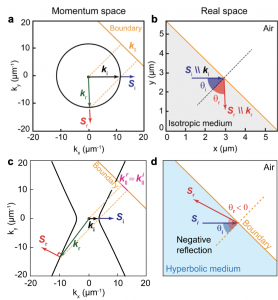
Fig. 1. Geometrical optics of polaritons: reflection. (a) Reflection of isotropic polaritons upon momentum conservation at the boundary (![]() ). The black solid line represents the polaritonic IFC, where ki,r and Si,r are always parallel. (b) Real-space illustration of reflection of isotropic polaritons. The angle of reflection θr is always equal to that of incidence θi (specular reflection). (c) Negative reflection of hyperbolic polaritons upon momentum conservation at the boundary (
). The black solid line represents the polaritonic IFC, where ki,r and Si,r are always parallel. (b) Real-space illustration of reflection of isotropic polaritons. The angle of reflection θr is always equal to that of incidence θi (specular reflection). (c) Negative reflection of hyperbolic polaritons upon momentum conservation at the boundary (![]() ). The black solid line represents the IFC of hyperbolic polaritons. ki,r and Si,r, generally non-collinear, indicate the wavefronts and Poynting vectors of the incident/reflected hyperbolic polaritons, respectively. (d) Real-space illustration of negative reflection of hyperbolic polaritons. The angle of reflection θr is negative, and Si and Sr are on the same side of the normal to the boundary. Adapted from Álvarez-Pérez et al. (2022).
). The black solid line represents the IFC of hyperbolic polaritons. ki,r and Si,r, generally non-collinear, indicate the wavefronts and Poynting vectors of the incident/reflected hyperbolic polaritons, respectively. (d) Real-space illustration of negative reflection of hyperbolic polaritons. The angle of reflection θr is negative, and Si and Sr are on the same side of the normal to the boundary. Adapted from Álvarez-Pérez et al. (2022).
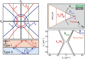
Fig. 2. Geometrical optics of polaritons: refraction. (Top left) Schematic showing qy = 0 cuts of the polariton IFCs in isotropic and hyperbolic media. The group velocities vA,B and their tilt angles θA > 0, θB < 0 are indicated. Adapted from Sternbach et al. (2023). (Bottom left) Schematic of the polariton rays at an interface between a hyperbolic and an isotropic medium. Adapted from Sternbach et al. (2023). (Top right) Schematics of a refractive hyperbolic lens between two hyperbolic media. The top and bottom boundaries of the lens have the same slope as the boundary in the bottom right panel. Upon refraction at the boundaries (orange contour line), polaritons converge at a focal spot (red dot). Sin and kin display the direction of propagation and the wavevector of incident polaritons. Adapted from Duan et al. (2021). (Bottom right) Analytic IFCs of polaritons in two hyperbolic media. The boundary is nearly perpendicular to the asymptote of the hyperbolic IFC, and thus refracted polaritons propagate almost parallel to the boundary with large wavevectors. Adapted from Duan et al. (2021).
Helical plasmon polaritons
Helical plasmon polaritons: were predicted to form in topologically nontrivial Weyl semimetals (Pellegrino, Katsnelson, and Polini 2015). Plasmon polariton dispersion may enable the detection of a chiral anomaly: a charge imbalance between the Weyl nodes in the presence of electric and magnetic fields (Zhou, Chang, and Xiao 2015). The Fermi surface of Weyl semimental features open disjoint segments – the Fermi arcs – associated with the topolical surface states. The resulting Fermi arc plasmon polaritons are predicted to be chiral and to reveal unidirectional propagation (Song and Rudner 2017). Helical plasmon terminology was also applied to describe one-dimensional plasmon polaritons associated with the helical state in domain walls of topologically nontrivial conductors including anomalous quantum Hall systems (Iorsh, Rahmanova, and Titov 2019). Helicity-dependence of plasmon polaritons is discussed in the context of unidirectional propagation in plasmonic meta-structures controlled by the circular polarization of light (J. Lin et al. 2013; Huang et al. 2013; Hopfield 1958).
Hopfield polaritons
Hopfield polaritons: a bold theoretical concept of light-matter hybridization proposed by John Hopfield in his doctoral thesis back in 1958 (Ref. (Hopfield 1958)). Hopfield also co-authored the first experimental paper on polaritons devoted to the study of phonon polariton dispersion in GaP by means of Raman scattering (Henry and Hopfield 1965). Other early contributions to the theory of polaritons (short of introducing this term) were made by Fano (Fano 1956), Huang (HUANG 1951) and Tolpygo (Tolpygo 1950).
Hybrid polaritons
Hyperbolic polaritons
Hyperbolic polaritons. Anisotropic media are predicted to support an interesting class of polaritonic light-matter modes referred to as “hyperbolic” because their iso-frequency surface is a hyperboloid (Kumar et al. 2015; Poddubny et al. 2013; J. S. Gomez-Diaz and Alù 2016; J. Sebastian Gomez-Diaz, Tymchenko, and Alù 2015; Caldwell et al. 2014; Guo et al. 2012; Cortes et al. 2012; J. Sun, Litchinitser, and Zhou 2014; Narimanov and Kildishev 2015a). These modes exist over a range of frequencies where the in-plane permittivity and the out-of-plane (c-axis) permittivity are of the opposite sign. Hyperbolic electrodynamics and hyperbolic polaritons can originate from a variety of physical processes including phonons (T. G. Folland et al. 2018; Caldwell et al. 2014; S. Dai et al. 2014; Giles et al. 2018; Taboada-Gutiérrez et al. 2020; Caldwell et al. 2019; Fali et al. 2019; Ambrosio et al. 2017; Ambrosio et al. 2018; G. Hu, Shen, et al. 2020; Siyuan Dai, Quan, et al. 2019; Siyuan Dai, Tymchenko, Xu, et al. 2018) inter-subband transitions in quantum wells (Hoffman et al. 2009; Feng et al. 2017; Lu et al. 2018) plasmons (Poddubny et al. 2013; J. Sun, Litchinitser, and Zhou 2014; Iorsh et al. 2013; Narimanov and Kildishev 2015b; G. Hu, Krasnok, et al. 2020; C. Wang et al. 2020) excitons (Epstein et al. 2020) and Cooper pairs (see Cooper pair polaritons). Hyperbolic polaritons dramatically enhance the local photonic density of states and are predicted to give rise to strong nonlinearities (Rivera et al. 2017). Hyperbolic polaritons enable canalization imaging (Belov and Hao 2006) with image effectively transferred by high-momentum sub-diffractional polaritonic rays from back to front surface of the polaritonic medium (Peining Li et al. 2020; S. Dai, Ma, Andersen, et al. 2015; Correas-Serrano, Alù, and Gomez-Diaz 2017; Peining Li et al. 2015).
Image Polaritons
Image polaritons: virtual polariton modes produced by image charges at the interface of a polaritonic medium and a metal. Lee et al. have experimentally demonstrated low loss response of image polaritons at the interface of hBN separated with a thin spacer from a metallic substrate (I.-H. Lee et al. 2020) (Fig.5D).
Interband Polaritons
Interband polaritons. The matter constituent of these polaritons originates from contributions of the optical response associated with transitions across the energy gap in the electronic spectrum of a material. These include transitions across the energy gap in semiconductors (Stahl 1979) and superconductors or transitions involving mini-bands/flat-bands in moire superlattices of van der Waals materials (Tomadin, Guinea, and Polini 2014; Ni et al. 2015; Hesp et al. 2019; Novelli et al. 2020) (see also Moire polaritons). The frequency dependence of s2(w)xw, where s2(w) is the imaginary part of the complex conductivity, is informative for the analysis of interband polaritons (D. N. Basov et al. 1995; Ni et al. 2015). Spectra of s2(w)xw reveal a series of steps separated by plateaus, with each step uncovering the energy scale associated with separate interband contributions. In the limit of wà 0, the product s2(w)xw quantifies the spectral weight of intraband processes to the plasmon polaritons. Interband effects play a central role in theoretical proposals for the implementation of population inversion (Wolff 1970), gain and superluminal plasmon polaritons (Low, Chen, and Basov 2018).
Intersubband Polaritons
Intersubband polaritons. Dini et al. reported the first experimental observation of the vacuum-field Rabi splitting of an intersubband transition inside a planar microcavity hosting two-dimensional electron gas (Dini et al. 2003; Dario Ballarini and De Liberato 2019). Nonlinearities associated with intesubband transitions in semiconductors can be dramatically enhanced by in hybrid structure with plasmonic metasurfaces (J. Lee, Tymchenko, et al. 2014)(see also hybrid polaritons).
Josephson Plasmon Polariton
Kane Polaritons
Kane polaritons: surface plasmon polaritons formed with Kane quasiparticles. Kane polaritons were recently observed in pump-probe experiments on narrow gap II-VI semiconductors (Charnukha et al. 2019).
Landau Polaritons
Landau polaritons. The matter component of Landau polaritons originates from cyclotron resonances and transitions between quantized Landau levels relevant in low-dimensional electron gases subjected to high magnetic fields (X. Li et al. 2018; Paravicini-Bagliani et al. 2019). See also magneto-plasmon polariton.
Luttinger Liquid Polaritons
Luttinger liquid polaritons: plasmon polaritons in one-dimensional conductors recently revealed by infrared nano-imaging of single- and multiple-wall carbon nanotubes (Z. Shi et al. 2015). Interacting electrons confined in one dimension are generally described by the Luttinger liquid formalism (Luttinger 1963; Haldane 1981). Anomalous dependence of the plasmonic quality factor on gate voltage was interpreted in terms of plasmon-plasmon interaction in carbon nano-tubes (S. Wang et al. 2020).
Magnon Polaritons
Magnon polaritons. The matter constituent of these polaritons originate from antiferromagnetic (Camley 1980; Camley and Mills 1982) and ferromagnetic resonances. In weak magnetic fields surface magnon polaritons are predicted to acquire non-reciprocal properties. Macedo and Camley analyzed the propagation of surface magnon polaritons in anisotropic antiferromagnets (Macêdo and Camley 2019). Sloan et al. predicted that surface magnon polaritons will strongly enhance the spin relaxation of quantum emitters in the proximity of antiferromagnetic materials such as MnF2 or FeF2 (Ref. (Sloan et al. 2019). Kruk et al. developed artificial structures with hyperbolic magnetic response with principal components of the magnetic permeability tensor having the opposite signs (Kruk et al. 2016). Magnetic materials also support hybrid polaritons, including hybrid magnon-phonon polaritons recently observed in ErFeO3/LiNbO3 multilayers (Sivarajah et al. 2019).
Magneto-Plasmon Polaritons
Microcavity Polaritons
Moire Polaritons
Molecular Polaritons
Molecular polaritons. Organic semiconductors and molecules embedded in optical (nano)cavities under strong and ultrastrong coupling promote the dynamical formation of molecular polaritons: hybrid energy eigenstates composed of entangled photonic, electronic, and vibrational degrees of freedom (Javani and Stockman 2016; Herrera and Owrutsky 2020; J. P. Long and Simpkins 2015). Molecular polaritons were demonstrated to enhance energy transfer (Xiang et al. 2020) and DC conductivity (Orgiu et al. 2015). Progress with nano-structures enabled a demonstration of the strong-light matter coupling with a single molecule embedded in a plasmonic cavity (Chikkaraddy et al. 2016). Molecular polaritons enable control of optical nonlinarities via manipulations of cavity characteristics (Xiang et al. 2019). Molecular polaritons can form hybrid polaritons by coupling to surface plasmons (Memmi et al. 2017), for example. We remark that molecular polaritons are commonly reffered to as vibrational polaritons.
Mott Polaritons(QED)
Mott polaritons (QED): non-equilibrium driven states in an array of circuit QED cavities or optical resonators (Henriet et al. 2014; S. Schmidt and Koch 2013). See also polaritonic lattices.
Mott Polaritons (QM)
Mott polaritons (QM) were also introduced in context of the resonant coupling between strongly correlated electrons in solid Mott insulators integrated in a single-mode cavity (Kiffner et al. 2019).
Negative reflection and refraction of polaritons at the nanoscale
Gonzalo Álvarez-Pérez and Pablo Alonso-González
Department of Physics, University of Oviedo, Oviedo 33006, Spain.
Center of Research on Nanomaterials and Nanotechnology CINN (CSIC-Universidad de Oviedo), El Entrego 33940, Spain.
Reflection and refraction stand out as two of the most fundamental optical phenomena. Reflection, the process by which light bounces off objects, serves as the foundation for the design of mirrors and cavities. Conversely, refraction involves the bending of light as it traverses different media, setting the basis for the design of lenses and prisms. Investigating reflection and refraction at the nanoscale is imperative to understand how light interacts with matter and to develop innovative nano-optical devices, the primary focus of the field of nano-optics.
Within this context, polaritons can showcase unconventional optical behaviors, such as anomalous or negative refraction and reflection. Anomalous refraction manifests when light deviates unexpectedly as it traverses different media. Refraction is deemed “negative” if the refracted beam emerges on the same side of the interface normal as the incident one (Fig. 1), offering potential applications in superlenses that beat the diffraction limit of light and enable high-resolution imaging. On the other hand, negative reflection is characterized by light being reflected towards the same side of the boundary’s normal on which it is incident, opening avenues for unconventional optical devices like nanoresonators with high density of optical states or cloaking materials, capable of manipulating light flow to render objects invisible or redirect light around them.
Originally, negative reflection was observed for free-space light reflecting off artificially engineered interfaces (metasurfaces) (Yu et al., 2011; Aieta et al., 2012; Liu et al., 2016; Liu et al., 2018; Gérardin et al., 2019) and chiral mirrors (Zhang et al., 2007), while negative refraction was initially demonstrated in artificial metamaterials and superlattices with simultaneous negative permittivity ε and permeability μ (Shelby et al., 2001; Pimenov et al., 2005). However, these platforms preclude the direct, real-space visualization of the phenomenon, as not only low optical losses but also an adequate material platform are required to guarantee a clear real-space visualization of negative refraction and reflection.
In this regard, polar dielectrics with extreme anisotropy have emerged in the last decade as a highly promising platform for studying anomalous instances of reflection and refraction. Due to the strong lattice anisotropy, these materials can host hyperbolic phonon polaritons in the mid- and far- infrared (mid-, far-IR) (Galiffi et al., 2024). The propagation of such hyperbolic polaritons is highly counter-intuitive, primarily due to the misalignment between the direction of propagation and the direction of the wavefronts. This non-collinearity, together with conservation of momentum (see section “Geometrical optics of polaritons”), allows hyperbolic polaritons to exhibit anomalous refraction and reflection phenomena.
Giles et al. (2016) demonstrated anomalous reflection in nanocones of hexagonal boron nitride (hBN), while Álvarez-Pérez et al. (2022) presented the initial visualization of negative reflection of nanoscale-confined polaritons by fabricating subwavelength mirrors in alpha-phase molybdenum trioxide (α-MoO3). They found that the wavevector of the outcoming wave, kr, can be much greater in modulus than that of incidence ki, implying that the reflected wave can exhibit a much smaller wavelength. Based on this, they introduced the design of a nanoresonator for in-plane hyperbolic polaritons, significantly enhancing the intensity.
Furthermore, Duan et al. (2021) reported the visualization of anomalous refraction of polaritons at the nanoscale by fabricating nanoprisms in a substrate underneath α-MoO3. They also introduced the design of the first planar refractive lens for polaritons, achieving a focus size 50 times smaller than the wavelength of the incident light. More recently, Hu et al. (2023) used α-MoO3 with a graphene overlayer to demonstrate in-plane negative refraction of polaritons at the interface, showing gate tunability. Sternbach et al. (2023) employed α-MoO3/hBN bicrystals to reveal negative refraction of mid-IR polaritons for propagation normal to the interface. Zhang et al. (2022) independently studied negative reflection and refraction of anisotropic polaritons from a theoretical point of view.
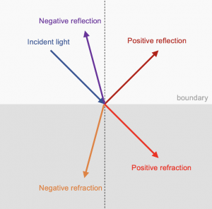
Fig. 1. Negative reflection and refraction. Schematics showing the directions of positive and negative reflection and refraction at an arbitrary interface.
Phonon Polaritons
Plasmon Polaritons
Plasmon polaritons: probably the most thoroughly studied class of polaritons. A surface plasmon polariton is a transverse magnetic (TM)-polarized optical surface wave that, for example, propagates along a flat metal-dielectric interface, typically at visible or infrared wavelengths (Zayats, Smolyaninov, and Maradudin 2005; Maier 2007; Gramotnev and Bozhevolnyi 2010). Plasmon polaritons have rich implications for technology (Atwater and Polman 2010; Berini and De Leon 2012; Bogdanov, Boltasseva, and Shalaev 2019; J. Lee, Jung, et al. 2014). Nonlinear (Kauranen and Zayats 2012; Nookala et al. 2016; Tymchenko et al. 2015) and quantum (Z. Jacob and Shalaev 2011; Tame et al. 2013; Bozhevolnyi and Khurgin 2017; Fakonas, Mitskovets, and Atwater 2015; Dheur et al. 2016) properties of plasmonic structures are in the vanguard of current research. Plasmon-polaritons can be controlled at femto-second time scales (Wagner, Fei, et al. 2014; Charnukha et al. 2019; Wagner, McLeod, et al. 2014; MacDonald et al. 2009; Eisele et al. 2014; M. A. Huber et al. 2017), enabling access to novel physics and applications (Yao et al. 2020; Krasavin, Zayats, and Zheludev 2005). Plasmonic waveguides have been incorporated with light-emitting materials, paving the way for integrated plasmonic and photonic structures (J. Shi et al. 2017). Plasmon-polaritons have been harnessed to implement high-quality factors such as whispering gallery microcavities (B. Min et al. 2009). In parallel, many research groups are searching for new plasmonic media with the properties optimized for different classes of plasmonic effects (Boltasseva and Atwater 2011; Naik, Shalaev, and Boltasseva 2013; F. Xia et al. 2014; da Jornada et al. 2020). Van der Waals materials, and especially graphene, are emerging as outstanding plasmonic media in light of their inherent tunability with different stimuli (see Dirac plasmons). Acoustic plasmon polaritons are a special example of hybrid polaritons whose frequency-momentum w(q) dispersion is predicted to be linear (Hwang and Das Sarma 2009; Principi, Asgari, and Polini 2011; Profumo et al. 2012; S. Chen et al. 2017; Stauber and Gómez-Santos 2012). Acoustic plasmon plaritons have been demonstrated (I.-H. Lee et al. 2019; Pablo Alonso-González et al. 2017; Lundeberg et al. 2017) in structures where graphene resides in close proximity to metallic surfaces. Spoof surface plasmons polaritons were introduced describe plasmon polaritons on the surface of artificial metallic structures and metamaterials (Pendry, Martín-Moreno, and Garcia-Vidal 2004). Airy surface plasmon polaritons are the surface counterparts of non-diffracting airy waves (Berry and Balazs 1979) and have been demonstrated by direct nano-imaging (Minovich et al. 2011). Chiral plasmon polaritons (Hentschel et al. 2017) were predicted to occur in twisted bilayer graphene (Stauber, Low, and Gómez-Santos 2018).
Plexcitons
Plexcitons are a specific example of hybrid polaritons. The matter constituent of plexcitons originates from plasmon-exciton coupled modes (Vasa et al. 2013; Fofang et al. 2008; Fofang et al. 2011; Manjavacas, García de Abajo, and Nordlander 2011; Yuen-Zhou et al. 2016; Manuel et al. 2019; K. Wu et al. 2013). Historically, plexciton studies have focused primarily on localized states (Fofang et al. 2008; Törmä and Barnes 2015). Propagating plexciton states also exist and offer potential for compact quantum information carriers a well as opportunities for mediating emitter-emitter coupling (Gonçalves et al. 2018; Karanikolas, Thanopulos, and Paspalakis 2019; Chervy et al. 2018). Composite structures and multilayers can feature plexcitons. An interesting recent example of plexciton study has been conducted in the setting of scanning probe nano-optical imaging and spectroscopy (Fig.8). This work by May et al (May et al. 2020) along with a study by Groß et al. (Groß et al. 2018) implemented the scanning optical cavities formed between a nano-optical antenna and the substrate. The authors investigated CdSe/ZnS quantum dots using this scanning cavity approach and observed plexitonic Rabi splitting of 163 meV.
Polaritons Parametric Amplification
Polaritons parametric amplification, gain and lasing have been demonstrated for exciton polaritons in microcavities (Savvidis et al. 2000; Saba et al. 2001; S. Kéna-Cohen and Forrest 2010; Deng et al. 2003). Resonant coupling between photons and excitons in microcavities can efficiently generate significant single-pass optical gains. Polaritonic lasing has been implemented and analyzed in different material systems hosting plasmon polartions and exciton polaritons (Yuanda Liu et al. 2019). Amplification of demons (Zhiyuan Sun, Basov, and Fogler 2016) has been predicted as well but is yet to be experimentally demonstrated.
Polaritonic Chemistry
Polaritonic chemistry: an emerging field focused on modifying pathways of chemical reactions in molecular systems coupled to photonic cavities (Flick, Rivera, and Narang 2018; Hutchison et al. 2012; Yuen-Zhou and Menon 2019; Flick et al. 2017; Schäfer et al. 2020).
Polaritonic Circuits
Polaritonic circuits, devices, arrays and systems. Both light and matter constituents of polaritons are amenable to controls with external stimuli (Sanvitto and Kéna-Cohen 2016). The use of exciton polaritons as building blocks for future information processing such as spin-switches (A. Amo et al. 2010),spin-memory (Gao et al. 2012), transistors (D. Ballarini et al. 2013), logic gates (Antón et al. 2013), resonant tunneling diodes (Nguyen et al. 2013), routers (Marsault et al. 2015), lasers (Kavokin et al. 2016) has recently been demonstrated. The first polaritonic systems are also emerging and include quantum simulators and networks for neuromorphic computers (Dario Ballarini et al. 2020). Transition metal dichalcogenide material WSe2, integrated into microcavity devices acts as efficient light emitting device (Gu et al. 2019).
Polaritonic Lattices and Quantum Simulators
Polaritonic lattices and quantum simulators. A variety of experimental approaches have been utilized to implement one- and two-dimensional arrays of interacting polaritons. In the field of microcavity exciton polaritons gate arrays, spatially dependent optical potential as well as surface acoustic waves (Cerda-Méndez et al. 2010), have been utilized to generate arrays/lattices (Alberto Amo and Bloch 2016). One-dimensional exciton polariton superlattices reveal weak lasing assigned to a novel type of a phase transition in this interacting system (L. Zhang et al. 2015). Arrays of evanescently-coupled cavities hosting neutral atoms (M.J. Hartmann, Brandão, and Plenio 2008) have been proposed as quantum simulators (QS), where the photon blockade provided by the atom limits the occupancy of each cavity to one, allowing for the implementation of the Bose-Hubbard model. QSs require controllable quantum systems that efficiently simulate a Hamiltonian of interest, which may encode phases with a significant degree of entanglement and is not amenable to calculations by classical computer (N. Y. Kim and Yamamoto 2017; Georgescu, Ashhab, and Nori 2014; Cirac and Zoller 2012; Bloch, Dalibard, and Nascimbène 2012; N. C. Harris et al. 2017; Aspuru-Guzik and Walther 2012). Lattices of exciton polaritons (N. Y. Kim and Yamamoto 2017; Michael J. Hartmann, Brandão, and Plenio 2006; Greentree et al. 2006; Byrnes, Recher, and Yamamoto 2010; Na and Yamamoto 2010; Berloff et al. 2017), have emerged as a promising platform for QS, along with ultracold atoms (Bloch, Dalibard, and Nascimbène 2012; Esslinger 2010), trapped ions (Blatt and Roos 2012; K Kim et al. 2011; Britton et al. 2012), and superconducting circuits (Houck, Türeci, and Koch 2012; Koch et al. 2010). Moire superlattices of plasmon polaritons (Figure 6) present yet another example of polaritonic lattices. Moire superlattices were realized in graphene devices with nanostructured gate electrodes (Xiong et al. 2019) as well as in moire superlattices of twisted graphene layers (Yankowitz et al. 2012).
Polaritonic interference refraction, collimation, front shaping and waveguiding
Polariton-polariton interactions
Polaron Polaritons
Polaron-polaritons. In TMDC monolayers, the itinerant electrons dynamically screen exciton to form new quasiparticle branches — the attractive and repulsive polaron — each with a renormalized mass and energy (Sidler et al. 2017; Efimkin and MacDonald 2017). Microcavity polaritons with the matter constituent linked to these polaron branches are referred to as polaron-polaritons (Sidler et al. 2017).
Quantum Hall Polaritons
Quantum Hall polaritons are a product of coupling cavity photons to the cyclotron resonance excitations of electron liquids in high-mobility semiconductor quantum wells or graphene sheets (Scalari et al. 2012; Pellegrino et al. 2016). The edge channels of the quantum Hall effect offer a platform for probing interference and entanglement effects in the setting of a condensed matter system since the edge states propagation is ballistic, one-dimensional, and chiral. This platform enables experimental implementation of electron quantum optics (Neder et al. 2007; Bäuerle et al. 2018; Splettstoesser and Haug 2017; Glattli and Roulleau 2017) and may be suitable for the realization of flying qubits. In a parallel development, Smolka et al. (Smolka et al. 2014) investigated cavity exciton polaritons in the presence of high-mobility 2D electron gas subjected to external magnetic field and discovered novel correlated electron phases Knuppel et al. (Knüppel et al. 2019) reported on strong polariton polariton interactions in the fractional quantum Hall regime.
Rydberg Polaritons (QED)
Rydberg polaritons (QED): photons dressed by highly excited atomic Rydberg states under conditions of electromagnetic induced transparency. These polaritons can either reside in a cavity or propagate throughout an atomic ensemble. In a cavity, Rydberg dressing bestows an atomic ensemble with the character of a two-level system: the excitation of a single Rydberg polariton prevents the creation of a second one, in the so-called “Rydberg blockade” regime. Under conditions of electromagnetic induced transparency, polaritons can propagate within an optically-dense atomic cloud. These polaritons can then be made to interact with each other via Rydberg dressing: the first Rydberg polariton alters the transparency condition for the second one, preventing its propagation within a certain “blockade radius” (Lukin et al. 2001; Comparat and Pillet 2010; Gorshkov et al. 2011; Shahmoon et al. 2011). Rydberg polaritons are appealing for quantum logic functionalities (Peyronel et al. 2012) and for realizing synthetic materials via many-body states of light (Carusotto and Ciuti 2013; Clark et al. 2019).
Rydberg Polaritons (QM)
Rydberg polaritons (QM): a special example of exciton polaritons with matter constituent associated with strongly interacting Rydberg states of excitons (Walther, Johne, and Pohl 2018). Candidate systems include TMDC monolayers (Chernikov et al. 2014) and cuprous oxide, where Rydberg states with principal quantum numbers of up to n = 25 are feasible (Merkl et al. 2020).
Soliton Polaritons
Soliton polaritons. Propagating wavepackets in semiconductor micorcavities are referred to as soliton polaritons (Fig.10 C). In quantum optics, topological soliton polaritons refer to composite objects made of fermions trapped in an optical soliton. The prototypical one-dimensional (1D) model of solitons posessing nontrivial topology is the model of Su-Schrieffer-Heeger (SSH) chains (Su, Schrieffer, and Heeger 1979). Variants of the SSH Hamiltonian have been emulated in the 1D lattices of microcavity exciton polaritons (St-Jean et al. 2017) and also in the system of quantum emitters coupled to a photonic waveguide (Bello et al. 2019). Topological phases of polritons in cavity waveguides were analysed in Ref. (Downing et al. 2019).
Spin Polaritons
Spin polaritons: this term was coined in the context of polariton microcavity diode lasers operating via injection of spin polarized currents (Bhattacharya et al. 2017).
Spin Plasmon Polaritons
Transformation Optics with Polaritons
Transformation optics with polaritons. Transformation optics refers to a general principle for designing a complex electromagnetic medium with tailored properties by carefully crafting the spatial patterns of the local optical index (Pendry, Schurig, and Smith 2006; Leonhardt 2006). This general principle has been extended to polaritons (Huidobro et al. 2010) and polartonic cavities (Ginis et al. 2012), and specifically to plasmon polaritons in graphene (Vakil and Engheta 2011). Losses present the most significant experimental roadblock for practical transformational polaritonics. Recent advances with highly confined but low-loss plasmon polaritons (Ni et al. 2018) and phonon-polaritons (Caldwell et al. 2014) fulfill important experimental preconditions for the realization of transformation optics ideas in polaritonic systems.
Tamm Surface Plasmon Polaritons
Tamm surface plasmon polaritons are associated with Tamm states at metallic surfaces (Tamm 1932). Common surface plasmon polaritons are formed with a TM (transverse magnetic) polarization at the boundary of metallic and dielectric surfaces and lie to the right of the light cone. Tamm polaritons are found with both TM and TE (transverse electric) polarizations and their dispersion can be within the light cone (Kaliteevski et al. 2007; B. Liu, Wu, and Menon 2019).
Trion Polaritons
Trion polaritons. The matter constituent of these polaritons is formed by charged excitons or trions (see also charged polaritons). Trion polaritons are commonly found in the response of TMDC semiconductors (Dhara et al. 2018; Emmanuele et al. 2020) and also in carbon nanotubes (Möhl et al. 2018).
Tunneling Plasmon Polaritons
Tunneling plasmon polaritons were predicted (de Vega and García de Abajo 2017) and observed (Woessner et al. 2017) in an atomically thick tunable quantum tunnelling devices consisting of two layers of graphene separated by 1 nm of h-BN. By applying a bias voltage between the graphene layers one creates an electron gas coupled to a hole gas. Even though the total charge of the devices is zero, this system supports propagating graphene plasmons.
Valley Polaritons
Valley polaritons. The matter constituent of these polaritons originates from valley polarized excitons in TMDC semiconductors (Fig.4B and exciton polaritons). The electronic structure of two-dimensional TMDC semiconductors endows this class of materials with the spin–valley degree of freedom that provides an optically accessible route for the control and manipulation of electron spin (Xu et al. 2014; Peng et al. 2020; Guddala et al. 2019).
Vibrational polaritons
Wannier or Wannier-Mott Polaritons
Wannier or Wannier-Mott polaritons borrow their matter part from Wannier excitons in semiconductors (Egri and Stahl 1979).
Waveguides and photonic crystals for polaritons
Waveguides and photonic crystals for polaritons. Waveguides and photonic crystals allow one to design and control the properties of photons, and thus of polaritons, both in quantum optics and quantum materials. In waveguide QED, different type of emitters (neutral atoms, quantum dots, color centers, superconducting qubits) are coupled to a one-dimensional (1D) optical channels (Asenjo-Garcia, Hood, et al. 2017), such as fibers (Vetsch et al. 2010; Goban et al. 2012), photonic crystals (Goban et al. 2015; Hood et al. 2016), and transmission lines (Mirhosseini et al. 2019; Yanbing Liu and Houck 2017) (Cavity quantum electrodynamics and cavity polaritons and Fig.11 A). Channel with a band gap give rise to atom-photon bound states (i.e., polaritonic bound states) provided the atomic resonance frequency is close to the band edge. Beyond the band-edge, photons are bound to the atoms, forming localized polaritonic cavities that can be harnessed for realizing quantum simulation and quantum information processing (Cavity quantum electrodynamics and cavity polaritons). If the coupling between photons and atoms is strong enough, bound states emerge even if the atomic resonance frequency lies inside the band (i.e., as a “bound states in the continuum”) due to multiple scattering (Calajó et al. 2016; T. Shi et al. 2016). In the field of quantum materials, photonic-crystals structures were fabricated using common phonon-polariton oxide systems LiTaO3 and LiNbO3 (Fig. 11B). Pump-probe experiments in Fig. 11B revealed the key attributes of the dispersion control by these periodic structures. A significant deficiency of conventional photonic crystals is that they do not allow for dynamical dispersion engineering. Xiong et al. circumvented this limitation and demonstrated a broadly tunable two-dimensional photonic crystal for surface plasmon polaritons [cross-ref-xiond]. Infrared nano-imaging revealed the formation of a photonic bandgap and an artificial domain wall which supports highly confined one-dimensional plasmonic modes.
Zenneck-Sommerfeld waves and Norton waves
Zenneck-Sommerfeld waves and Norton waves: an early example of a guided electromagnetic wave at the interface of media with negative and positive dielectric function Refs. (Zenneck 1907; Norton 1936; Sommerfeld 1909) the same condition that is required for the formation of polaritonic modes in THz, infrared and optical frequencies. The original prediction of Zenneck-Sommerfeld waves pertained to the radiofrequency wave at the interface of air and the earth. In this analysis the surface of the Earth was regarded as a lossy dielectric. The concept of Zenneck-Sommerfeld waves and closely related Norton waves has been applied to a broad class of wave patterns on the surface of metallic (Sarrazin and Vigneron 2005; Sihvola, Jiaran Qi, and Lindell 2010; Michalski and Mosig 2015; A Yu Nikitin et al. 2009) and dielectric materials (Babicheva et al. 2018).
Acknowledgements
We thank Tristin Rice for his technical assistance in the organization and upkeep of references and figures as well as for his contributions in formatting, structure, and style of the Polariton Panorama.
[1] D. N. Basov, M. M. Fogler, and F. J. García de Abajo, “Polaritons in van der Waals materials,” Science (1979), vol. 354, no. 6309, Oct. 2016, doi: 10.1126/science.aag1992.
[2] D. N. Basov, R. D. Averitt, and D. Hsieh, “Towards properties on demand in quantum materials,” Nat Mater, vol. 16, no. 11, pp. 1077–1088, Nov. 2017, doi: 10.1038/nmat5017.
[3] T. Low et al., “Polaritons in layered two-dimensional materials,” Nat Mater, vol. 16, no. 2, pp. 182–194, Feb. 2017, doi: 10.1038/nmat4792.
[4] D. E. Chang, J. S. Douglas, A. González-Tudela, C.-L. Hung, and H. J. Kimble, “Colloquium : Quantum matter built from nanoscopic lattices of atoms and photons,” Rev Mod Phys, vol. 90, no. 3, p. 031002, Aug. 2018, doi: 10.1103/RevModPhys.90.031002.
[5] A. A. Clerk, K. W. Lehnert, P. Bertet, J. R. Petta, and Y. Nakamura, “Hybrid quantum systems with circuit quantum electrodynamics,” Nat Phys, vol. 16, no. 3, pp. 257–267, Mar. 2020, doi: 10.1038/s41567-020-0797-9.
[6] I. Carusotto, A. A. Houck, A. J. Kollár, P. Roushan, D. I. Schuster, and J. Simon, “Photonic materials in circuit quantum electrodynamics,” Nat Phys, vol. 16, no. 3, pp. 268–279, Mar. 2020, doi: 10.1038/s41567-020-0815-y.
[7] M. Ruggenthaler, N. Tancogne-Dejean, J. Flick, H. Appel, and A. Rubio, “From a quantum-electrodynamical light–matter description to novel spectroscopies,” Nat Rev Chem, vol. 2, no. 3, p. 0118, Mar. 2018, doi: 10.1038/s41570-018-0118.
[8] P. Forn-Díaz, L. Lamata, E. Rico, J. Kono, and E. Solano, “Ultrastrong coupling regimes of light-matter interaction,” Rev Mod Phys, vol. 91, no. 2, p. 025005, Jun. 2019, doi: 10.1103/RevModPhys.91.025005.
[9] S. McArdle, S. Endo, A. Aspuru-Guzik, S. C. Benjamin, and X. Yuan, “Quantum computational chemistry,” Rev Mod Phys, vol. 92, no. 1, p. 015003, Mar. 2020, doi: 10.1103/RevModPhys.92.015003.
[10] A. Frisk Kockum, A. Miranowicz, S. de Liberato, S. Savasta, and F. Nori, “Ultrastrong coupling between light and matter,” Nature Reviews Physics, vol. 1, no. 1, pp. 19–40, Jan. 2019, doi: 10.1038/s42254-018-0006-2.
[11] R. Jestädt, M. Ruggenthaler, M. J. T. Oliveira, A. Rubio, and H. Appel, “Light-matter interactions within the Ehrenfest–Maxwell–Pauli–Kohn–Sham framework: fundamentals, implementation, and nano-optical applications,” Adv Phys, vol. 68, no. 4, pp. 225–333, Oct. 2019, doi: 10.1080/00018732.2019.1695875.
[12] Z. M. Raines, A. A. Allocca, M. Hafezi, and V. M. Galitski, “Cavity Higgs polaritons,” Phys Rev Res, vol. 2, no. 1, p. 013143, Feb. 2020, doi: 10.1103/PhysRevResearch.2.013143.
[13] Z. Sun, M. M. Fogler, D. N. Basov, and A. J. Millis, “Collective modes and terahertz near-field response of superconductors,” Phys Rev Res, vol. 2, no. 2, p. 023413, Jun. 2020, doi: 10.1103/PhysRevResearch.2.023413.
[14] P. B. Littlewood and C. M. Varma, “Gauge-Invariant Theory of the Dynamical Interaction of Charge Density Waves and Superconductivity,” Phys Rev Lett, vol. 47, no. 11, pp. 811–814, Sep. 1981, doi: 10.1103/PhysRevLett.47.811.
[15] L. R. Walker, “Magnetostatic Modes in Ferromagnetic Resonance,” Physical Review, vol. 105, no. 2, pp. 390–399, Jan. 1957, doi: 10.1103/PhysRev.105.390.
[16] A. A. Allocca, Z. M. Raines, J. B. Curtis, and V. M. Galitski, “Cavity superconductor-polaritons,” Phys Rev B, vol. 99, no. 2, p. 020504, Jan. 2019, doi: 10.1103/PhysRevB.99.020504.
[17] Z. Sun and A. J. Millis, “Bardasis-Schrieffer polaritons in excitonic insulators,” Phys Rev B, vol. 102, no. 4, p. 041110, Jul. 2020, doi: 10.1103/PhysRevB.102.041110.
[18] H. T. Stinson et al., “Imaging the nanoscale phase separation in vanadium dioxide thin films at terahertz frequencies,” Nat Commun, vol. 9, no. 1, p. 3604, Dec. 2018, doi: 10.1038/s41467-018-05998-5.
[19] N. G. Basov, “Semiconductor Lasers,” Science (1979), vol. 149, no. 3686, pp. 821–827, Aug. 1965, doi: 10.1126/science.149.3686.821.
[20] H. Deng, H. Haug, and Y. Yamamoto, “Exciton-polariton Bose-Einstein condensation,” Rev Mod Phys, vol. 82, no. 2, pp. 1489–1537, May 2010, doi: 10.1103/RevModPhys.82.1489.
[21] T. Schwartz, J. A. Hutchison, C. Genet, and T. W. Ebbesen, “Reversible Switching of Ultrastrong Light-Molecule Coupling,” Phys Rev Lett, vol. 106, no. 19, p. 196405, May 2011, doi: 10.1103/PhysRevLett.106.196405.
[22] S. Kéna-Cohen, S. A. Maier, and D. D. C. Bradley, “Ultrastrongly Coupled Exciton-Polaritons in Metal-Clad Organic Semiconductor Microcavities,” Adv Opt Mater, vol. 1, no. 11, pp. 827–833, Nov. 2013, doi: 10.1002/adom.201300256.
[23] L. Tian and H. J. Carmichael, “Quantum trajectory simulations of two-state behavior in an optical cavity containing one atom,” Phys Rev A (Coll Park), vol. 46, no. 11, pp. R6801–R6804, Dec. 1992, doi: 10.1103/PhysRevA.46.R6801.
[24] A. Imamoḡlu, H. Schmidt, G. Woods, and M. Deutsch, “Strongly Interacting Photons in a Nonlinear Cavity,” Phys Rev Lett, vol. 79, no. 8, pp. 1467–1470, Aug. 1997, doi: 10.1103/PhysRevLett.79.1467.
[25] X. Liu et al., “Strong light–matter coupling in two-dimensional atomic crystals,” Nat Photonics, vol. 9, no. 1, pp. 30–34, Jan. 2015, doi: 10.1038/nphoton.2014.304.
[26] J. Šik, M. Schubert, T. Hofmann, and V. Gottschalch, “Free-carrier effects and optical phonons in GaNAs/GaAs superlattice heterostructures measured by infrared spectroscopic ellipsometry,” MRS Internet Journal of Nitride Semiconductor Research, vol. 5, no. 1, p. e3, Jun. 2000, doi: 10.1557/S109257830000003X.
[27] E. L. Runnerstrom, K. P. Kelley, E. Sachet, C. T. Shelton, and J.-P. Maria, “Epsilon-near-Zero Modes and Surface Plasmon Resonance in Fluorine-Doped Cadmium Oxide Thin Films,” ACS Photonics, vol. 4, no. 8, pp. 1885–1892, Aug. 2017, doi: 10.1021/acsphotonics.7b00429.
[28] K. P. Kelley et al., “Multiple Epsilon-Near-Zero Resonances in Multilayered Cadmium Oxide: Designing Metamaterial-Like Optical Properties in Monolithic Materials,” ACS Photonics, vol. 6, no. 5, pp. 1139–1145, May 2019, doi: 10.1021/acsphotonics.9b00367.
[29] A. Alù, M. G. Silveirinha, A. Salandrino, and N. Engheta, “Epsilon-near-zero metamaterials and electromagnetic sources: Tailoring the radiation phase pattern,” Phys Rev B, vol. 75, no. 15, p. 155410, Apr. 2007, doi: 10.1103/PhysRevB.75.155410.
[30] M. H. Javani and M. I. Stockman, “Real and Imaginary Properties of Epsilon-Near-Zero Materials,” Phys Rev Lett, vol. 117, no. 10, p. 107404, Sep. 2016, doi: 10.1103/PhysRevLett.117.107404.
[31] T. G. Folland, G. Lu, A. Bruncz, J. R. Nolen, M. Tadjer, and J. D. Caldwell, “Vibrational Coupling to Epsilon-Near-Zero Waveguide Modes,” ACS Photonics, vol. 7, no. 3, pp. 614–621, Mar. 2020, doi: 10.1021/acsphotonics.0c00071.
[32] I. Liberal, A. M. Mahmoud, Y. Li, B. Edwards, and N. Engheta, “Photonic doping of epsilon-near-zero media,” Science (1979), vol. 355, no. 6329, pp. 1058–1062, Mar. 2017, doi: 10.1126/science.aal2672.
[33] L. Shi and J. C. W. Song, “Plasmon Geometric Phase and Plasmon Hall Shift,” Phys Rev X, vol. 8, no. 2, p. 021020, Apr. 2018, doi: 10.1103/PhysRevX.8.021020.
[34] A. Kumar, A. Nemilentsau, K. H. Fung, G. Hanson, N. X. Fang, and T. Low, “Chiral plasmon in gapped Dirac systems,” Phys Rev B, vol. 93, no. 4, p. 041413, Jan. 2016, doi: 10.1103/PhysRevB.93.041413.
[35] J. C. W. Song and M. S. Rudner, “Chiral plasmons without magnetic field,” Proceedings of the National Academy of Sciences, vol. 113, no. 17, pp. 4658–4663, Apr. 2016, doi: 10.1073/pnas.1519086113.
[36] M. J. Bhaseen, M. Hohenadler, A. O. Silver, and B. D. Simons, “Polaritons and Pairing Phenomena in Bose-Hubbard Mixtures,” Phys Rev Lett, vol. 102, no. 13, p. 135301, Mar. 2009, doi: 10.1103/PhysRevLett.102.135301.
[37] H. Hübener et al., “Engineering quantum materials with chiral optical cavities,” Nat Mater, vol. 20, no. 4, pp. 438–442, Apr. 2021, doi: 10.1038/s41563-020-00801-7.
[38] V. D. Vaidya et al., “Tunable-Range, Photon-Mediated Atomic Interactions in Multimode Cavity QED,” Phys Rev X, vol. 8, no. 1, p. 011002, Jan. 2018, doi: 10.1103/PhysRevX.8.011002.
[39] N. Jia et al., “A strongly interacting polaritonic quantum dot,” Nat Phys, vol. 14, no. 6, pp. 550–554, Jun. 2018, doi: 10.1038/s41567-018-0071-6.
[40] S. Faure et al., “Relaxation and emission of Bragg-mode and cavity-mode polaritons in a ZnO microcavity at room temperature,” Appl Phys Lett, vol. 95, no. 12, p. 121102, Sep. 2009, doi: 10.1063/1.3232228.
[41] S. Donati et al., “Twist of generalized skyrmions and spin vortices in a polariton superfluid,” Proceedings of the National Academy of Sciences, vol. 113, no. 52, pp. 14926–14931, Dec. 2016, doi: 10.1073/pnas.1610123114.
[42] D. Goldberg et al., “Exciton-lattice polaritons in multiple-quantum-well-based photonic crystals,” Nat Photonics, vol. 3, no. 11, pp. 662–666, Nov. 2009, doi: 10.1038/nphoton.2009.190.
[43] E. S. Sedov, I. V. Iorsh, S. M. Arakelian, A. P. Alodjants, and A. Kavokin, “Hyperbolic Metamaterials with Bragg Polaritons,” Phys Rev Lett, vol. 114, no. 23, p. 237402, Jun. 2015, doi: 10.1103/PhysRevLett.114.237402.
[44] C. Weisbuch, M. Nishioka, A. Ishikawa, and Y. Arakawa, “Observation of the coupled exciton-photon mode splitting in a semiconductor quantum microcavity,” Phys Rev Lett, vol. 69, no. 23, pp. 3314–3317, Dec. 1992, doi: 10.1103/PhysRevLett.69.3314.
[45] C. Weisbuch and H. Benisty, “Microcavities in Ecole Polytechnique Fédérale de Lausanne, Ecole Polytechnique (France) and elsewhere: past, present and future,” physica status solidi (b), vol. 242, no. 11, pp. 2345–2356, Sep. 2005, doi: 10.1002/pssb.200560972.
[46] V. M. Agranovich, M. Litinskaia, and D. G. Lidzey, “Cavity polaritons in microcavities containing disordered organic semiconductors,” Phys Rev B, vol. 67, no. 8, p. 085311, Feb. 2003, doi: 10.1103/PhysRevB.67.085311.
[47] P. G. Savvidis, J. J. Baumberg, R. M. Stevenson, M. S. Skolnick, D. M. Whittaker, and J. S. Roberts, “Angle-Resonant Stimulated Polariton Amplifier,” Phys Rev Lett, vol. 84, no. 7, pp. 1547–1550, Feb. 2000, doi: 10.1103/PhysRevLett.84.1547.
[48] R. M. Stevenson et al., “Continuous Wave Observation of Massive Polariton Redistribution by Stimulated Scattering in Semiconductor Microcavities,” Phys Rev Lett, vol. 85, no. 17, pp. 3680–3683, Oct. 2000, doi: 10.1103/PhysRevLett.85.3680.
[49] H. Deng, G. Weihs, C. Santori, J. Bloch, and Y. Yamamoto, “Condensation of Semiconductor Microcavity Exciton Polaritons,” Science (1979), vol. 298, no. 5591, pp. 199–202, Oct. 2002, doi: 10.1126/science.1074464.
[50] T. Guillet and C. Brimont, “Polariton condensates at room temperature,” C R Phys, vol. 17, no. 8, pp. 946–956, Oct. 2016, doi: 10.1016/j.crhy.2016.07.002.
[51] Á. Cuevas et al., “First observation of the quantized exciton-polariton field and effect of interactions on a single polariton,” Sci Adv, vol. 4, no. 4, Apr. 2018, doi: 10.1126/sciadv.aao6814.
[52] A. Delteil, T. Fink, A. Schade, S. Höfling, C. Schneider, and A. İmamoğlu, “Towards polariton blockade of confined exciton–polaritons,” Nat Mater, vol. 18, no. 3, pp. 219–222, Mar. 2019, doi: 10.1038/s41563-019-0282-y.
[53] G. Muñoz-Matutano et al., “Emergence of quantum correlations from interacting fibre-cavity polaritons,” Nat Mater, vol. 18, no. 3, pp. 213–218, Mar. 2019, doi: 10.1038/s41563-019-0281-z.
[54] S. S. Demirchyan, I. Yu. Chestnov, A. P. Alodjants, M. M. Glazov, and A. V. Kavokin, “Qubits Based on Polariton Rabi Oscillators,” Phys Rev Lett, vol. 112, no. 19, p. 196403, May 2014, doi: 10.1103/PhysRevLett.112.196403.
[55] I. v. Novikov and A. A. Maradudin, “Channel polaritons,” Phys Rev B, vol. 66, no. 3, p. 035403, Jun. 2002, doi: 10.1103/PhysRevB.66.035403.
[56] S. I. Bozhevolnyi, V. S. Volkov, E. Devaux, J.-Y. Laluet, and T. W. Ebbesen, “Channel plasmon subwavelength waveguide components including interferometers and ring resonators,” Nature, vol. 440, no. 7083, pp. 508–511, Mar. 2006, doi: 10.1038/nature04594.
[57] P. A. D. Gonçalves, S. Xiao, N. M. R. Peres, and N. A. Mortensen, “Hybridized Plasmons in 2D Nanoslits: From Graphene to Anisotropic 2D Materials,” ACS Photonics, vol. 4, no. 12, pp. 3045–3054, Dec. 2017, doi: 10.1021/acsphotonics.7b00558.
[58] Z. Fei et al., “Gate-tuning of graphene plasmons revealed by infrared nano-imaging,” Nature, vol. 487, no. 7405, pp. 82–85, Jul. 2012, doi: 10.1038/nature11253.
[59] J. Chen et al., “Optical nano-imaging of gate-tunable graphene plasmons,” Nature, vol. 487, no. 7405, pp. 77–81, Jul. 2012, doi: 10.1038/nature11254.
[60] M. D. Goldflam et al., “Tuning and Persistent Switching of Graphene Plasmons on a Ferroelectric Substrate,” Nano Lett, vol. 15, no. 8, pp. 4859–4864, Aug. 2015, doi: 10.1021/acs.nanolett.5b00125.
[61] S. Xiao, X. Zhu, B.-H. Li, and N. A. Mortensen, “Graphene-plasmon polaritons: From fundamental properties to potential applications,” Front Phys (Beijing), vol. 11, no. 2, p. 117801, Apr. 2016, doi: 10.1007/s11467-016-0551-z.
[62] M. Wagner et al., “Ultrafast and Nanoscale Plasmonic Phenomena in Exfoliated Graphene Revealed by Infrared Pump–Probe Nanoscopy,” Nano Lett, vol. 14, no. 2, pp. 894–900, Feb. 2014, doi: 10.1021/nl4042577.
[63] D. J. Rizzo et al., “Graphene/$\alpha$-RuCl$_3$: An Emergent 2D Plasmonic Interface,” Jul. 2020, doi: 10.1021/acs.nanolett.0c03466.
[64] F. Wen et al., “Charge Transfer Plasmons: Optical Frequency Conductances and Tunable Infrared Resonances,” ACS Nano, vol. 9, no. 6, pp. 6428–6435, Jun. 2015, doi: 10.1021/acsnano.5b02087.
[65] M. Förg et al., “Cavity-control of interlayer excitons in van der Waals heterostructures,” Nat Commun, vol. 10, no. 1, p. 3697, Dec. 2019, doi: 10.1038/s41467-019-11620-z.
[66] R. Rapaport, R. Harel, E. Cohen, A. Ron, E. Linder, and L. N. Pfeiffer, “Negatively Charged Quantum Well Polaritons in a <math display=”inline”> <mi>GaAs</mi> <mi>/</mi> <mi>AlAs</mi> </math> Microcavity: An Analog of Atoms in a Cavity,” Phys Rev Lett, vol. 84, no. 7, pp. 1607–1610, Feb. 2000, doi: 10.1103/PhysRevLett.84.1607.
[67] J. M. Raimond and S. Haroche, Confined Electrons and Photons, vol. 340. Boston, MA: Springer US, 1995. doi: 10.1007/978-1-4615-1963-8.
[68] A. Tiene, J. Levinsen, M. M. Parish, A. H. MacDonald, J. Keeling, and F. M. Marchetti, “Extremely imbalanced two-dimensional electron-hole-photon systems,” Phys Rev Res, vol. 2, no. 2, p. 023089, Apr. 2020, doi: 10.1103/PhysRevResearch.2.023089.
[69] P. A. Cherenkov, “Visible Emission of Clean Liquids by Action of γ Radiation,” Dokl. Akad. Nauk SSSR 2, 451 (1934).
[70] P. Genevet, D. Wintz, A. Ambrosio, A. She, R. Blanchard, and F. Capasso, “Controlled steering of Cherenkov surface plasmon wakes with a one-dimensional metamaterial,” Nat Nanotechnol, vol. 10, no. 9, pp. 804–809, Sep. 2015, doi: 10.1038/nnano.2015.137.
[71] D. H. Auston, K. P. Cheung, J. A. Valdmanis, and D. A. Kleinman, “Cherenkov Radiation from Femtosecond Optical Pulses in Electro-Optic Media,” Phys Rev Lett, vol. 53, no. 16, pp. 1555–1558, Oct. 1984, doi: 10.1103/PhysRevLett.53.1555.
[72] C. Maciel-Escudero, A. Konečná, R. Hillenbrand, and J. Aizpurua, “Probing and steering bulk and surface phonon polaritons in uniaxial materials using fast electrons: Hexagonal boron nitride,” Phys Rev B, vol. 102, no. 11, p. 115431, Sep. 2020, doi: 10.1103/PhysRevB.102.115431.
[73] Y. Zhang et al., “Tunable Cherenkov Radiation of Phonon Polaritons in Silver Nanowire/Hexagonal Boron Nitride Heterostructures,” Nano Lett, vol. 20, no. 4, pp. 2770–2777, Apr. 2020, doi: 10.1021/acs.nanolett.0c00419.
[74] H. T. Stinson et al., “Infrared nanospectroscopy and imaging of collective superfluid excitations in anisotropic superconductors,” Phys Rev B, vol. 90, no. 1, p. 014502, Jul. 2014, doi: 10.1103/PhysRevB.90.014502.
[75] A. Dodel et al., “Cooper pair polaritons in cold fermionic atoms within a cavity,” Phys Rev Res, vol. 2, no. 1, p. 013184, Feb. 2020, doi: 10.1103/PhysRevResearch.2.013184.
[76] W. L. Barnes, A. Dereux, and T. W. Ebbesen, “Surface plasmon subwavelength optics,” Nature, vol. 424, no. 6950, pp. 824–830, Aug. 2003, doi: 10.1038/nature01937.
[77] P. J. Schuck, D. P. Fromm, A. Sundaramurthy, G. S. Kino, and W. E. Moerner, “Improving the Mismatch between Light and Nanoscale Objects with Gold Bowtie Nanoantennas,” Phys Rev Lett, vol. 94, no. 1, p. 017402, Jan. 2005, doi: 10.1103/PhysRevLett.94.017402.
[78] P. Biagioni, J.-S. Huang, and B. Hecht, “Nanoantennas for visible and infrared radiation,” Reports on Progress in Physics, vol. 75, no. 2, p. 024402, Feb. 2012, doi: 10.1088/0034-4885/75/2/024402.
[79] L. Novotny and N. van Hulst, “Antennas for light,” Nat Photonics, vol. 5, no. 2, pp. 83–90, Feb. 2011, doi: 10.1038/nphoton.2010.237.
[80] J. J. Baumberg, J. Aizpurua, M. H. Mikkelsen, and D. R. Smith, “Extreme nanophotonics from ultrathin metallic gaps,” Nat Mater, vol. 18, no. 7, pp. 668–678, Jul. 2019, doi: 10.1038/s41563-019-0290-y.
[81] M. Tamagnone et al., “Ultra-confined mid-infrared resonant phonon polaritons in van der Waals nanostructures,” Sci Adv, vol. 4, no. 6, Jun. 2018, doi: 10.1126/sciadv.aat7189.
[82] A. M. Dubrovkin, B. Qiang, T. Salim, D. Nam, N. I. Zheludev, and Q. J. Wang, “Resonant nanostructures for highly confined and ultra-sensitive surface phonon-polaritons,” Nat Commun, vol. 11, no. 1, p. 1863, Dec. 2020, doi: 10.1038/s41467-020-15767-y.
[83] L. v. Brown et al., “Nanoscale Mapping and Spectroscopy of Nonradiative Hyperbolic Modes in Hexagonal Boron Nitride Nanostructures,” Nano Lett, vol. 18, no. 3, pp. 1628–1636, Mar. 2018, doi: 10.1021/acs.nanolett.7b04476.
[84] X. Chen et al., “Modern Scattering‐Type Scanning Near‐Field Optical Microscopy for Advanced Material Research,” Advanced Materials, vol. 31, no. 24, p. 1804774, Jun. 2019, doi: 10.1002/adma.201804774.
[85] Z. Fei et al., “Infrared Nanoscopy of Dirac Plasmons at the Graphene–SiO 2 Interface,” Nano Lett, vol. 11, no. 11, pp. 4701–4705, Nov. 2011, doi: 10.1021/nl202362d.
[86] P. J. Schuck, A. Weber-Bargioni, P. D. Ashby, D. F. Ogletree, A. Schwartzberg, and S. Cabrini, “Life Beyond Diffraction: Opening New Routes to Materials Characterization with Next-Generation Optical Near-Field Approaches,” Adv Funct Mater, vol. 23, no. 20, pp. 2539–2553, May 2013, doi: 10.1002/adfm.201203432.
[87] S. Berweger, J. M. Atkin, R. L. Olmon, and M. B. Raschke, “Light on the Tip of a Needle: Plasmonic Nanofocusing for Spectroscopy on the Nanoscale,” J Phys Chem Lett, vol. 3, no. 7, pp. 945–952, Apr. 2012, doi: 10.1021/jz2016268.
[88] K.-D. Park, T. Jiang, G. Clark, X. Xu, and M. B. Raschke, “Radiative control of dark excitons at room temperature by nano-optical antenna-tip Purcell effect,” Nat Nanotechnol, vol. 13, no. 1, pp. 59–64, Jan. 2018, doi: 10.1038/s41565-017-0003-0.
[89] B.-Y. Jiang, L. M. Zhang, A. H. Castro Neto, D. N. Basov, and M. M. Fogler, “Generalized spectral method for near-field optical microscopy,” J Appl Phys, vol. 119, no. 5, p. 054305, Feb. 2016, doi: 10.1063/1.4941343.
[90] F. Keilmann and R. Hillenbrand, “Near-field microscopy by elastic light scattering from a tip,” Philosophical Transactions of the Royal Society of London. Series A: Mathematical, Physical and Engineering Sciences, vol. 362, no. 1817, pp. 787–805, Apr. 2004, doi: 10.1098/rsta.2003.1347.
[91] J. M. Atkin, S. Berweger, A. C. Jones, and M. B. Raschke, “Nano-optical imaging and spectroscopy of order, phases, and domains in complex solids,” Adv Phys, vol. 61, no. 6, pp. 745–842, Dec. 2012, doi: 10.1080/00018732.2012.737982.
[92] M. Fleischhauer, A. Imamoglu, and J. P. Marangos, “Electromagnetically induced transparency: Optics in coherent media,” Rev Mod Phys, vol. 77, no. 2, pp. 633–673, Jul. 2005, doi: 10.1103/RevModPhys.77.633.
[93] S. E. Harris, J. E. Field, and A. Imamoğlu, “Nonlinear optical processes using electromagnetically induced transparency,” Phys Rev Lett, vol. 64, no. 10, pp. 1107–1110, Mar. 1990, doi: 10.1103/PhysRevLett.64.1107.
[94] M. D. Lukin, “Colloquium : Trapping and manipulating photon states in atomic ensembles,” Rev Mod Phys, vol. 75, no. 2, pp. 457–472, Apr. 2003, doi: 10.1103/RevModPhys.75.457.
[95] H. Zoubi and H. Ritsch, “Lifetime and emission characteristics of collective electronic excitations in two-dimensional optical lattices,” Phys Rev A (Coll Park), vol. 83, no. 6, p. 063831, Jun. 2011, doi: 10.1103/PhysRevA.83.063831.
[96] R. J. Bettles, S. A. Gardiner, and C. S. Adams, “Cooperative eigenmodes and scattering in one-dimensional atomic arrays,” Phys Rev A (Coll Park), vol. 94, no. 4, p. 043844, Oct. 2016, doi: 10.1103/PhysRevA.94.043844.
[97] A. Asenjo-Garcia, M. Moreno-Cardoner, A. Albrecht, H. J. Kimble, and D. E. Chang, “Exponential Improvement in Photon Storage Fidelities Using Subradiance and ‘Selective Radiance’ in Atomic Arrays,” Phys Rev X, vol. 7, no. 3, p. 031024, Aug. 2017, doi: 10.1103/PhysRevX.7.031024.
[98] E. Shahmoon, D. S. Wild, M. D. Lukin, and S. F. Yelin, “Cooperative Resonances in Light Scattering from Two-Dimensional Atomic Arrays,” Phys Rev Lett, vol. 118, no. 11, p. 113601, Mar. 2017, doi: 10.1103/PhysRevLett.118.113601.
[99] D. Pines, “ELECTRON INTERACTION IN SOLIDS,” Can J Phys, vol. 34, no. 12A, pp. 1379–1394, Dec. 1956, doi: 10.1139/p56-154.
[100] Z. Sun, D. N. Basov, and M. M. Fogler, “Universal linear and nonlinear electrodynamics of a Dirac fluid,” Proceedings of the National Academy of Sciences, vol. 115, no. 13, pp. 3285–3289, Mar. 2018, doi: 10.1073/pnas.1717010115.
[101] Z. Sun, D. N. Basov, and M. M. Fogler, “Adiabatic Amplification of Plasmons and Demons in 2D Systems,” Phys Rev Lett, vol. 117, no. 7, p. 076805, Aug. 2016, doi: 10.1103/PhysRevLett.117.076805.
[102] M. Jablan, H. Buljan, and M. Soljačić, “Plasmonics in graphene at infrared frequencies,” Phys Rev B, vol. 80, no. 24, p. 245435, Dec. 2009, doi: 10.1103/PhysRevB.80.245435.
[103] A. Woessner et al., “Highly confined low-loss plasmons in graphene–boron nitride heterostructures,” Nat Mater, vol. 14, no. 4, pp. 421–425, Apr. 2015, doi: 10.1038/nmat4169.
[104] G. X. Ni et al., “Fundamental limits to graphene plasmonics,” Nature, vol. 557, no. 7706, pp. 530–533, May 2018, doi: 10.1038/s41586-018-0136-9.
[105] M. I. D’yakono, “New type of electromagnetic wave propagating at an interface,” Sov. Phys., 1988.
[106] O. Takayama, L. Crasovan, D. Artigas, and L. Torner, “Observation of Dyakonov Surface Waves,” Phys Rev Lett, vol. 102, no. 4, p. 043903, Jan. 2009, doi: 10.1103/PhysRevLett.102.043903.
[107] Z. Jacob and E. E. Narimanov, “Optical hyperspace for plasmons: Dyakonov states in metamaterials,” Appl Phys Lett, vol. 93, no. 22, p. 221109, Dec. 2008, doi: 10.1063/1.3037208.
[108] S. Dai et al., “Manipulation and Steering of Hyperbolic Surface Polaritons in Hexagonal Boron Nitride,” Advanced Materials, vol. 30, no. 16, p. 1706358, Apr. 2018, doi: 10.1002/adma.201706358.
[109] F. J. Alfaro-Mozaz et al., “Nanoimaging of resonating hyperbolic polaritons in linear boron nitride antennas,” Nat Commun, vol. 8, no. 1, p. 15624, Aug. 2017, doi: 10.1038/ncomms15624.
[110] I. Dolado et al., “Nanoscale Guiding of Infrared Light with Hyperbolic Volume and Surface Polaritons in van der Waals Material Ribbons,” Advanced Materials, vol. 32, no. 9, p. 1906530, Mar. 2020, doi: 10.1002/adma.201906530.
[111] D. B. Mast, A. J. Dahm, and A. L. Fetter, “Observation of Bulk and Edge Magnetoplasmons in a Two-Dimensional Electron Fluid,” Phys Rev Lett, vol. 54, no. 15, pp. 1706–1709, Apr. 1985, doi: 10.1103/PhysRevLett.54.1706.
[112] V. A. Volkov and S. A. Mikhailov, “Edge magnetoplasmons: low frequency weakly damped excitations in inhomogeneous two-dimensional electron systems,” Radio Engineering and Electronics Institute, USSR Academy of Sciences, 1988.
[113] N. Kumada et al., “Resonant Edge Magnetoplasmons and Their Decay in Graphene,” Phys Rev Lett, vol. 113, no. 26, p. 266601, Dec. 2014, doi: 10.1103/PhysRevLett.113.266601.
[114] I. Petković, F. I. B. Williams, and D. C. Glattli, “Edge magnetoplasmons in graphene,” J Phys D Appl Phys, vol. 47, no. 9, p. 094010, Mar. 2014, doi: 10.1088/0022-3727/47/9/094010.
[115] M. L. Sadowski, G. Martinez, M. Potemski, C. Berger, and W. A. de Heer, “Landau Level Spectroscopy of Ultrathin Graphite Layers,” Phys Rev Lett, vol. 97, no. 26, p. 266405, Dec. 2006, doi: 10.1103/PhysRevLett.97.266405.
[116] Z. Jiang et al., “Infrared Spectroscopy of Landau Levels of Graphene,” Phys Rev Lett, vol. 98, no. 19, p. 197403, May 2007, doi: 10.1103/PhysRevLett.98.197403.
[117] M. Orlita et al., “Carrier Scattering from Dynamical Magnetoconductivity in Quasineutral Epitaxial Graphene,” Phys Rev Lett, vol. 107, no. 21, p. 216603, Nov. 2011, doi: 10.1103/PhysRevLett.107.216603.
[118] Z.-G. Chen et al., “Observation of an intrinsic bandgap and Landau level renormalization in graphene/boron-nitride heterostructures,” Nat Commun, vol. 5, no. 1, p. 4461, Dec. 2014, doi: 10.1038/ncomms5461.
[119] I. O. Nedoliuk, S. Hu, A. K. Geim, and A. B. Kuzmenko, “Colossal infrared and terahertz magneto-optical activity in a two-dimensional Dirac material,” Nat Nanotechnol, vol. 14, no. 8, pp. 756–761, Aug. 2019, doi: 10.1038/s41565-019-0489-8.
[120] Z. Fei et al., “Edge and Surface Plasmons in Graphene Nanoribbons,” Nano Lett, vol. 15, no. 12, pp. 8271–8276, Dec. 2015, doi: 10.1021/acs.nanolett.5b03834.
[121] A. Y. Nikitin et al., “Real-space mapping of tailored sheet and edge plasmons in graphene nanoresonators,” Nat Photonics, vol. 10, no. 4, pp. 239–243, Apr. 2016, doi: 10.1038/nphoton.2016.44.
[122] P. Li et al., “Optical Nanoimaging of Hyperbolic Surface Polaritons at the Edges of van der Waals Materials,” Nano Lett, vol. 17, no. 1, pp. 228–235, Jan. 2017, doi: 10.1021/acs.nanolett.6b03920.
[123] P. Berini, “Plasmon-polariton waves guided by thin lossy metal films of finite width: Bound modes of symmetric structures,” Phys Rev B, vol. 61, no. 15, pp. 10484–10503, Apr. 2000, doi: 10.1103/PhysRevB.61.10484.
[124] M. Lorente-Crespo, G. C. Ballesteros, C. Mateo-Segura, and C. García-Meca, “Edge-Plasmon Whispering-Gallery Modes in Nanoholes,” Phys Rev Appl, vol. 13, no. 2, p. 024050, Feb. 2020, doi: 10.1103/PhysRevApplied.13.024050.
[125] T. Rindzevicius et al., “Nanohole Plasmons in Optically Thin Gold Films,” The Journal of Physical Chemistry C, vol. 111, no. 3, pp. 1207–1212, Jan. 2007, doi: 10.1021/jp065942q.
[126] A. Degiron, H. J. Lezec, N. Yamamoto, and T. W. Ebbesen, “Optical transmission properties of a single subwavelength aperture in a real metal,” Opt Commun, vol. 239, no. 1–3, pp. 61–66, Sep. 2004, doi: 10.1016/j.optcom.2004.05.058.
[127] N. Liu et al., “Plasmonic analogue of electromagnetically induced transparency at the Drude damping limit,” Nat Mater, vol. 8, no. 9, pp. 758–762, Sep. 2009, doi: 10.1038/nmat2495.
[128] R. Taubert, M. Hentschel, J. Kästel, and H. Giessen, “Classical Analog of Electromagnetically Induced Absorption in Plasmonics,” Nano Lett, vol. 12, no. 3, pp. 1367–1371, Mar. 2012, doi: 10.1021/nl2039748.
[129] H. Yan, T. Low, F. Guinea, F. Xia, and P. Avouris, “Tunable Phonon-Induced Transparency in Bilayer Graphene Nanoribbons,” Nano Lett, vol. 14, no. 8, pp. 4581–4586, Aug. 2014, doi: 10.1021/nl501628x.
[130] S. Xia, X. Zhai, L. Wang, and S. Wen, “Plasmonically induced transparency in in-plane isotropic and anisotropic 2D materials,” Opt Express, vol. 28, no. 6, p. 7980, Mar. 2020, doi: 10.1364/OE.389573.
[131] V. Walther, R. Johne, and T. Pohl, “Giant optical nonlinearities from Rydberg excitons in semiconductor microcavities,” Nat Commun, vol. 9, no. 1, p. 1309, Dec. 2018, doi: 10.1038/s41467-018-03742-7.
[132] J.-M. Ménard et al., “Revealing the dark side of a bright exciton–polariton condensate,” Nat Commun, vol. 5, no. 1, p. 4648, Dec. 2014, doi: 10.1038/ncomms5648.
[133] Z. Sun et al., “Optical control of room-temperature valley polaritons,” Nat Photonics, vol. 11, no. 8, pp. 491–496, Aug. 2017, doi: 10.1038/nphoton.2017.121.
[134] L. V. Hau, S. E. Harris, Z. Dutton, and C. H. Behroozi, “Light speed reduction to 17 metres per second in an ultracold atomic gas,” Nature, vol. 397, no. 6720, pp. 594–598, Feb. 1999, doi: 10.1038/17561.
[135] O. Kocharovskaya, Y. Rostovtsev, and M. O. Scully, “Stopping Light via Hot Atoms,” Phys Rev Lett, vol. 86, no. 4, pp. 628–631, Jan. 2001, doi: 10.1103/PhysRevLett.86.628.
[136] M. Bajcsy, A. S. Zibrov, and M. D. Lukin, “Stationary pulses of light in an atomic medium,” Nature, vol. 426, no. 6967, pp. 638–641, Dec. 2003, doi: 10.1038/nature02176.
[137] J. Kasprzak et al., “Bose–Einstein condensation of exciton polaritons,” Nature, vol. 443, no. 7110, pp. 409–414, Sep. 2006, doi: 10.1038/nature05131.
[138] I. Carusotto and C. Ciuti, “Quantum fluids of light,” Rev Mod Phys, vol. 85, no. 1, pp. 299–366, Feb. 2013, doi: 10.1103/RevModPhys.85.299.
[139] T. Byrnes, N. Y. Kim, and Y. Yamamoto, “Exciton–polariton condensates,” Nat Phys, vol. 10, no. 11, pp. 803–813, Nov. 2014, doi: 10.1038/nphys3143.
[140] A. Griffin, D. W. Snoke, and S. Stringari, Bose-Einstein Condensation. Cambridge University Press, 1995. doi: 10.1017/CBO9780511524240.
[141] A. A. High et al., “Spontaneous coherence in a cold exciton gas,” Nature, vol. 483, no. 7391, pp. 584–588, Mar. 2012, doi: 10.1038/nature10903.
[142] D. Snoke, “Spontaneous Bose Coherence of Excitons and Polaritons,” Science (1979), vol. 298, no. 5597, pp. 1368–1372, Nov. 2002, doi: 10.1126/science.1078082.
[143] J. P. Eisenstein and A. H. MacDonald, “Bose–Einstein condensation of excitons in bilayer electron systems,” Nature, vol. 432, no. 7018, pp. 691–694, Dec. 2004, doi: 10.1038/nature03081.
[144] D. W. Snoke and J. Keeling, “The new era of polariton condensates,” Phys Today, vol. 70, no. 10, pp. 54–60, Oct. 2017, doi: 10.1063/PT.3.3729.
[145] Y. Sun et al., “Bose-Einstein Condensation of Long-Lifetime Polaritons in Thermal Equilibrium,” Phys Rev Lett, vol. 118, no. 1, p. 016602, Jan. 2017, doi: 10.1103/PhysRevLett.118.016602.
[146] G. Lerario et al., “Room-temperature superfluidity in a polariton condensate,” Nat Phys, vol. 13, no. 9, pp. 837–841, Sep. 2017, doi: 10.1038/nphys4147.
[147] Y. Fu, H. Zhu, J. Chen, M. P. Hautzinger, X.-Y. Zhu, and S. Jin, “Metal halide perovskite nanostructures for optoelectronic applications and the study of physical properties,” Nat Rev Mater, vol. 4, no. 3, pp. 169–188, Mar. 2019, doi: 10.1038/s41578-019-0080-9.
[148] A. T. Hanbicki, M. Currie, G. Kioseoglou, A. L. Friedman, and B. T. Jonker, “Measurement of high exciton binding energy in the monolayer transition-metal dichalcogenides WS2 and WSe2,” Solid State Commun, vol. 203, pp. 16–20, Feb. 2015, doi: 10.1016/j.ssc.2014.11.005.
[149] T. Cheiwchanchamnangij and W. R. L. Lambrecht, “Quasiparticle band structure calculation of monolayer, bilayer, and bulk MoS <math display=”inline”> <msub> <mrow/> <mn>2</mn> </msub> </math>,” Phys Rev B, vol. 85, no. 20, p. 205302, May 2012, doi: 10.1103/PhysRevB.85.205302.
[150] A. Ramasubramaniam, “Large excitonic effects in monolayers of molybdenum and tungsten dichalcogenides,” Phys Rev B, vol. 86, no. 11, p. 115409, Sep. 2012, doi: 10.1103/PhysRevB.86.115409.
[151] H.-P. Komsa and A. V. Krasheninnikov, “Effects of confinement and environment on the electronic structure and exciton binding energy of MoS <math display=”inline”> <msub> <mrow/> <mn>2</mn> </msub> </math> from first principles,” Phys Rev B, vol. 86, no. 24, p. 241201, Dec. 2012, doi: 10.1103/PhysRevB.86.241201.
[152] H. Min, R. Bistritzer, J.-J. Su, and A. H. MacDonald, “Room-temperature superfluidity in graphene bilayers,” Phys Rev B, vol. 78, no. 12, p. 121401, Sep. 2008, doi: 10.1103/PhysRevB.78.121401.
[153] M. M. Fogler, L. V. Butov, and K. S. Novoselov, “High-temperature superfluidity with indirect excitons in van der Waals heterostructures,” Nat Commun, vol. 5, no. 1, p. 4555, Dec. 2014, doi: 10.1038/ncomms5555.
[154] F.-C. Wu, F. Xue, and A. H. MacDonald, “Theory of two-dimensional spatially indirect equilibrium exciton condensates,” Phys Rev B, vol. 92, no. 16, p. 165121, Oct. 2015, doi: 10.1103/PhysRevB.92.165121.
[155] A. V. Nalitov et al., “Optically trapped polariton condensates as semiclassical time crystals,” Phys Rev A (Coll Park), vol. 99, no. 3, p. 033830, Mar. 2019, doi: 10.1103/PhysRevA.99.033830.
[156] M. D. Fraser, S. Höfling, and Y. Yamamoto, “Physics and applications of exciton–polariton lasers,” Nat Mater, vol. 15, no. 10, pp. 1049–1052, Oct. 2016, doi: 10.1038/nmat4762.
[157] A. Gianfrate et al., “Superluminal X-waves in a polariton quantum fluid,” Light Sci Appl, vol. 7, no. 1, pp. 17119–17119, Jan. 2018, doi: 10.1038/lsa.2017.119.
[158] A. Gabbay, Y. Preezant, E. Cohen, B. M. Ashkinadze, and L. N. Pfeiffer, “Fermi Edge Polaritons in a Microcavity Containing a High Density Two-Dimensional Electron Gas,” Phys Rev Lett, vol. 99, no. 15, p. 157402, Oct. 2007, doi: 10.1103/PhysRevLett.99.157402.
[159] D. Pimenov, J. von Delft, L. Glazman, and M. Goldstein, “Fermi-edge exciton-polaritons in doped semiconductor microcavities with finite hole mass,” Phys Rev B, vol. 96, no. 15, p. 155310, Oct. 2017, doi: 10.1103/PhysRevB.96.155310.
[160] M. Baeten and M. Wouters, “Mahan polaritons and their lifetime due to hole recoil,” The European Physical Journal D, vol. 69, no. 11, p. 243, Nov. 2015, doi: 10.1140/epjd/e2015-60401-4.
[161] G. D. Mahan, “Excitons in Degenerate Semiconductors,” Physical Review, vol. 153, no. 3, pp. 882–889, Jan. 1967, doi: 10.1103/PhysRev.153.882.
[162] G. D. Mahan, “Excitons in Metals: Infinite Hole Mass,” Physical Review, vol. 163, no. 3, pp. 612–617, Nov. 1967, doi: 10.1103/PhysRev.163.612.
[163] T. Oka and S. Kitamura, “Floquet Engineering of Quantum Materials,” Annu Rev Condens Matter Phys, vol. 10, no. 1, pp. 387–408, Mar. 2019, doi: 10.1146/annurev-conmatphys-031218-013423.
[164] L. W. Clark, N. Jia, N. Schine, C. Baum, A. Georgakopoulos, and J. Simon, “Interacting Floquet polaritons,” Nature, vol. 571, no. 7766, pp. 532–536, Jul. 2019, doi: 10.1038/s41586-019-1354-5.
[165] F. Mahmood et al., “Selective scattering between Floquet–Bloch and Volkov states in a topological insulator,” Nat Phys, vol. 12, no. 4, pp. 306–310, Apr. 2016, doi: 10.1038/nphys3609.
[166] H. Hübener, U. De Giovannini, and A. Rubio, “Phonon Driven Floquet Matter,” Nano Lett, vol. 18, no. 2, pp. 1535–1542, Feb. 2018, doi: 10.1021/acs.nanolett.7b05391.
[167] F. J. Bezares et al., “Intrinsic Plasmon–Phonon Interactions in Highly Doped Graphene: A Near-Field Imaging Study,” Nano Lett, vol. 17, no. 10, pp. 5908–5913, Oct. 2017, doi: 10.1021/acs.nanolett.7b01603.
[168] D. Yoo et al., “Ultrastrong plasmon–phonon coupling via epsilon-near-zero nanocavities,” Nat Photonics, vol. 15, no. 2, pp. 125–130, Feb. 2021, doi: 10.1038/s41566-020-00731-5.
[169] S. Betzold et al., “Coherence and Interaction in Confined Room-Temperature Polariton Condensates with Frenkel Excitons,” ACS Photonics, vol. 7, no. 2, pp. 384–392, Feb. 2020, doi: 10.1021/acsphotonics.9b01300.
[170] D. G. Lidzey, D. D. C. Bradley, M. S. Skolnick, T. Virgili, S. Walker, and D. M. Whittaker, “Strong exciton–photon coupling in an organic semiconductor microcavity,” Nature, vol. 395, no. 6697, pp. 53–55, Sep. 1998, doi: 10.1038/25692.
[171] J. Keeling and S. Kéna-Cohen, “Bose–Einstein Condensation of Exciton-Polaritons in Organic Microcavities,” Annu Rev Phys Chem, vol. 71, no. 1, pp. 435–459, Apr. 2020, doi: 10.1146/annurev-physchem-010920-102509.
[172] S. Foteinopoulou, G. C. R. Devarapu, G. S. Subramania, S. Krishna, and D. Wasserman, “Phonon-polaritonics: enabling powerful capabilities for infrared photonics,” Nanophotonics, vol. 8, no. 12, pp. 2129–2175, Oct. 2019, doi: 10.1515/nanoph-2019-0232.
[173] K. L. Kliewer and R. Fuchs, “Optical Modes of Vibration in an Ionic Crystal Slab Including Retardation. I. Nonradiative Region,” Physical Review, vol. 144, no. 2, pp. 495–503, Apr. 1966, doi: 10.1103/PhysRev.144.495.
[174] A. Huber, N. Ocelic, D. Kazantsev, and R. Hillenbrand, “Near-field imaging of mid-infrared surface phonon polariton propagation,” Appl Phys Lett, vol. 87, no. 8, p. 081103, Aug. 2005, doi: 10.1063/1.2032595.
[175] R. Hillenbrand, T. Taubner, and F. Keilmann, “Phonon-enhanced light–matter interaction at the nanometre scale,” Nature, vol. 418, no. 6894, pp. 159–162, Jul. 2002, doi: 10.1038/nature00899.
[176] J. D. Caldwell et al., “Low-Loss, Extreme Subdiffraction Photon Confinement via Silicon Carbide Localized Surface Phonon Polariton Resonators,” Nano Lett, vol. 13, no. 8, pp. 3690–3697, Aug. 2013, doi: 10.1021/nl401590g.
[177] T. E. Tiwald et al., “Carrier concentration and lattice absorption in bulk and epitaxial silicon carbide determined using infrared ellipsometry,” Phys Rev B, vol. 60, no. 16, pp. 11464–11474, Oct. 1999, doi: 10.1103/PhysRevB.60.11464.
[178] T. Taubner, D. Korobkin, Y. Urzhumov, G. Shvets, and R. Hillenbrand, “Near-Field Microscopy Through a SiC Superlens,” Science (1979), vol. 313, no. 5793, pp. 1595–1595, Sep. 2006, doi: 10.1126/science.1131025.
[179] W. J. Moore and R. T. Holm, “Infrared dielectric constant of gallium arsenide,” J Appl Phys, vol. 80, no. 12, pp. 6939–6942, Dec. 1996, doi: 10.1063/1.363818.
[180] F. M. D. Pellegrino, M. I. Katsnelson, and M. Polini, “Helicons in Weyl semimetals,” Phys Rev B, vol. 92, no. 20, p. 201407, Nov. 2015, doi: 10.1103/PhysRevB.92.201407.
[181] J. Zhou, H.-R. Chang, and D. Xiao, “Plasmon mode as a detection of the chiral anomaly in Weyl semimetals,” Phys Rev B, vol. 91, no. 3, p. 035114, Jan. 2015, doi: 10.1103/PhysRevB.91.035114.
[182] J. C. W. Song and M. S. Rudner, “Fermi arc plasmons in Weyl semimetals,” Phys Rev B, vol. 96, no. 20, p. 205443, Nov. 2017, doi: 10.1103/PhysRevB.96.205443.
[183] I. Iorsh, G. Rahmanova, and M. Titov, “Plasmon-Polariton from a Helical State in a Dirac Magnet,” ACS Photonics, vol. 6, no. 10, pp. 2450–2454, Oct. 2019, doi: 10.1021/acsphotonics.9b00683.
[184] J. Lin et al., “Polarization-controlled tunable directional coupling of surface plasmon polaritons,” Science (1979), vol. 340, no. 6130, pp. 331–334, 2013, doi: 10.1126/SCIENCE.1233746/SUPPL_FILE/LINSM.PDF.
[185] L. Huang et al., “Helicity dependent directional surface plasmon polariton excitation using a metasurface with interfacial phase discontinuity,” Light Sci Appl, vol. 2, no. 3, pp. e70–e70, Mar. 2013, doi: 10.1038/lsa.2013.26.
[186] J. J. Hopfield, “Theory of the Contribution of Excitons to the Complex Dielectric Constant of Crystals,” Physical Review, vol. 112, no. 5, pp. 1555–1567, Dec. 1958, doi: 10.1103/PhysRev.112.1555.
[187] C. H. Henry and J. J. Hopfield, “Raman Scattering by Polaritons,” Phys Rev Lett, vol. 15, no. 25, pp. 964–966, Dec. 1965, doi: 10.1103/PhysRevLett.15.964.
[188] U. Fano, “Atomic Theory of Electromagnetic Interactions in Dense Materials,” Physical Review, vol. 103, no. 5, pp. 1202–1218, Sep. 1956, doi: 10.1103/PhysRev.103.1202.
[189] K. HUANG, “Lattice Vibrations and Optical Waves in Ionic Crystals,” Nature, vol. 167, no. 4254, pp. 779–780, May 1951, doi: 10.1038/167779b0.
[190] K. B. Tolpygo, “Physical Properties of a rock salt lattice made up of deformeable ions,” Zh. Eksp. Teor, vol. 20, no. 6, 1950.
[191] J. D. Caldwell, I. Vurgaftman, J. G. Tischler, O. J. Glembocki, J. C. Owrutsky, and T. L. Reinecke, “Atomic-scale photonic hybrids for mid-infrared and terahertz nanophotonics,” Nat Nanotechnol, vol. 11, no. 1, pp. 9–15, Jan. 2016, doi: 10.1038/nnano.2015.305.
[192] L. Wendler and R. Haupt, “Long-range surface plasmon-phonon-polaritons,” Journal of Physics C: Solid State Physics, vol. 19, no. 11, pp. 1871–1896, Apr. 1986, doi: 10.1088/0022-3719/19/11/023.
[193] B. Askenazi et al., “Ultra-strong light–matter coupling for designer Reststrahlen band,” New J Phys, vol. 16, no. 4, p. 043029, Apr. 2014, doi: 10.1088/1367-2630/16/4/043029.
[194] M. Franckié, C. Ndebeka-Bandou, K. Ohtani, and J. Faist, “Quantum model of gain in phonon-polariton lasers,” Phys Rev B, vol. 97, no. 7, p. 075402, Feb. 2018, doi: 10.1103/PhysRevB.97.075402.
[195] N. C. Passler et al., “Strong Coupling of Epsilon-Near-Zero Phonon Polaritons in Polar Dielectric Heterostructures,” Nano Lett, vol. 18, no. 7, pp. 4285–4292, Jul. 2018, doi: 10.1021/acs.nanolett.8b01273.
[196] A. A. Strashko and V. M. Agranovich, “To the theory of surface plasmon-polaritons on metals covered with resonant thin films,” Opt Commun, vol. 332, pp. 201–205, Dec. 2014, doi: 10.1016/j.optcom.2014.06.069.
[197] D. C. Ratchford et al., “Controlling the Infrared Dielectric Function through Atomic-Scale Heterostructures,” ACS Nano, vol. 13, no. 6, pp. 6730–6741, Jun. 2019, doi: 10.1021/acsnano.9b01275.
[198] E. L. Runnerstrom et al., “Polaritonic Hybrid-Epsilon-near-Zero Modes: Beating the Plasmonic Confinement vs Propagation-Length Trade-Off with Doped Cadmium Oxide Bilayers,” Nano Lett, vol. 19, no. 2, pp. 948–957, Feb. 2019, doi: 10.1021/acs.nanolett.8b04182.
[199] K. Chaudhary et al., “Engineering phonon polaritons in van der Waals heterostructures to enhance in-plane optical anisotropy,” Sci Adv, vol. 5, no. 4, Apr. 2019, doi: 10.1126/sciadv.aau7171.
[200] S. Dai et al., “Graphene on hexagonal boron nitride as a tunable hyperbolic metamaterial,” Nat Nanotechnol, vol. 10, no. 8, pp. 682–686, Aug. 2015, doi: 10.1038/nnano.2015.131.
[201] A. Kumar, T. Low, K. H. Fung, P. Avouris, and N. X. Fang, “Tunable Light–Matter Interaction and the Role of Hyperbolicity in Graphene–hBN System,” Nano Lett, vol. 15, no. 5, pp. 3172–3180, May 2015, doi: 10.1021/acs.nanolett.5b01191.
[202] A. T. Costa, P. A. D. Gonçalves, D. N. Basov, F. H. L. Koppens, N. A. Mortensen, and N. M. R. Peres, “Harnessing ultraconfined graphene plasmons to probe the electrodynamics of superconductors,” Proceedings of the National Academy of Sciences, vol. 118, no. 4, Jan. 2021, doi: 10.1073/pnas.2012847118.
[203] H. Dehghani, Z. M. Raines, V. M. Galitski, and M. Hafezi, “Optical enhancement of superconductivity via targeted destruction of charge density waves,” Phys Rev B, vol. 101, no. 22, p. 224506, Jun. 2020, doi: 10.1103/PhysRevB.101.224506.
[204] D. Rodrigo et al., “Mid-infrared plasmonic biosensing with graphene,” Science (1979), vol. 349, no. 6244, pp. 165–168, Jul. 2015, doi: 10.1126/science.aab2051.
[205] M. Autore et al., “Boron nitride nanoresonators for phonon-enhanced molecular vibrational spectroscopy at the strong coupling limit,” Light Sci Appl, vol. 7, no. 4, pp. 17172–17172, Apr. 2018, doi: 10.1038/lsa.2017.172.
[206] C. R. Gubbin et al., “Hybrid longitudinal-transverse phonon polaritons,” Nat Commun, vol. 10, no. 1, p. 1682, Dec. 2019, doi: 10.1038/s41467-019-09414-4.
[207] T. G. Folland et al., “Reconfigurable infrared hyperbolic metasurfaces using phase change materials,” Nat Commun, vol. 9, no. 1, p. 4371, Dec. 2018, doi: 10.1038/s41467-018-06858-y.
[208] A. Poddubny, I. Iorsh, P. Belov, and Y. Kivshar, “Hyperbolic metamaterials,” Nat Photonics, vol. 7, no. 12, pp. 948–957, Dec. 2013, doi: 10.1038/nphoton.2013.243.
[209] J. S. Gomez-Diaz and A. Alù, “Flatland Optics with Hyperbolic Metasurfaces,” ACS Photonics, vol. 3, no. 12, pp. 2211–2224, Dec. 2016, doi: 10.1021/acsphotonics.6b00645.
[210] J. S. Gomez-Diaz, M. Tymchenko, and A. Alù, “Hyperbolic Plasmons and Topological Transitions Over Uniaxial Metasurfaces,” Phys Rev Lett, vol. 114, no. 23, p. 233901, Jun. 2015, doi: 10.1103/PhysRevLett.114.233901.
[211] J. D. Caldwell et al., “Sub-diffractional volume-confined polaritons in the natural hyperbolic material hexagonal boron nitride,” Nat Commun, vol. 5, no. 1, p. 5221, Dec. 2014, doi: 10.1038/ncomms6221.
[212] Y. Guo, W. Newman, C. L. Cortes, and Z. Jacob, “Applications of Hyperbolic Metamaterial Substrates,” Adv Optoelectron, vol. 2012, pp. 1–9, Dec. 2012, doi: 10.1155/2012/452502.
[213] C. L. Cortes, W. Newman, S. Molesky, and Z. Jacob, “Quantum nanophotonics using hyperbolic metamaterials,” Journal of Optics, vol. 14, no. 6, p. 063001, Jun. 2012, doi: 10.1088/2040-8978/14/6/063001.
[214] J. Sun, N. M. Litchinitser, and J. Zhou, “Indefinite by Nature: From Ultraviolet to Terahertz,” ACS Photonics, vol. 1, no. 4, pp. 293–303, Apr. 2014, doi: 10.1021/ph4000983.
[215] E. E. Narimanov and A. V. Kildishev, “Metamaterials: Naturally hyperbolic,” Nat Photonics, vol. 9, no. 4, pp. 214–216, Apr. 2015, doi: 10.1038/nphoton.2015.56.
[216] S. Dai et al., “Tunable Phonon Polaritons in Atomically Thin van der Waals Crystals of Boron Nitride,” Science (1979), vol. 343, no. 6175, pp. 1125–1129, Mar. 2014, doi: 10.1126/science.1246833.
[217] A. J. Giles et al., “Ultralow-loss polaritons in isotopically pure boron nitride,” Nat Mater, vol. 17, no. 2, pp. 134–139, Feb. 2018, doi: 10.1038/nmat5047.
[218] J. Taboada-Gutiérrez et al., “Broad spectral tuning of ultra-low-loss polaritons in a van der Waals crystal by intercalation,” Nat Mater, vol. 19, no. 9, pp. 964–968, Sep. 2020, doi: 10.1038/s41563-020-0665-0.
[219] J. D. Caldwell, I. Aharonovich, G. Cassabois, J. H. Edgar, B. Gil, and D. N. Basov, “Photonics with hexagonal boron nitride,” Nat Rev Mater, vol. 4, no. 8, pp. 552–567, Aug. 2019, doi: 10.1038/s41578-019-0124-1.
[220] A. Fali et al., “Refractive Index-Based Control of Hyperbolic Phonon-Polariton Propagation,” Nano Lett, vol. 19, no. 11, pp. 7725–7734, Nov. 2019, doi: 10.1021/acs.nanolett.9b02651.
[221] A. Ambrosio et al., “Mechanical Detection and Imaging of Hyperbolic Phonon Polaritons in Hexagonal Boron Nitride,” ACS Nano, vol. 11, no. 9, pp. 8741–8746, Sep. 2017, doi: 10.1021/acsnano.7b02323.
[222] A. Ambrosio et al., “Selective excitation and imaging of ultraslow phonon polaritons in thin hexagonal boron nitride crystals,” Light Sci Appl, vol. 7, no. 1, p. 27, Dec. 2018, doi: 10.1038/s41377-018-0039-4.
[223] G. Hu, J. Shen, C. Qiu, A. Alù, and S. Dai, “Phonon Polaritons and Hyperbolic Response in van der Waals Materials,” Adv Opt Mater, vol. 8, no. 5, p. 1901393, Mar. 2020, doi: 10.1002/adom.201901393.
[224] S. Dai et al., “Hyperbolic Phonon Polaritons in Suspended Hexagonal Boron Nitride,” Nano Lett, vol. 19, no. 2, pp. 1009–1014, Feb. 2019, doi: 10.1021/acs.nanolett.8b04242.
[225] S. Dai et al., “Internal Nanostructure Diagnosis with Hyperbolic Phonon Polaritons in Hexagonal Boron Nitride,” Nano Lett, vol. 18, no. 8, pp. 5205–5210, Aug. 2018, doi: 10.1021/acs.nanolett.8b02162.
[226] A. J. Hoffman et al., “Midinfrared semiconductor optical metamaterials,” J Appl Phys, vol. 105, no. 12, p. 122411, Jun. 2009, doi: 10.1063/1.3124087.
[227] K. Feng, G. Harden, D. L. Sivco, and A. J. Hoffman, “Subdiffraction Confinement in All-Semiconductor Hyperbolic Metamaterial Resonators,” ACS Photonics, vol. 4, no. 7, pp. 1621–1626, Jul. 2017, doi: 10.1021/acsphotonics.7b00309.
[228] D. Lu et al., “Nanostructuring Multilayer Hyperbolic Metamaterials for Ultrafast and Bright Green InGaN Quantum Wells,” Advanced Materials, vol. 30, no. 15, p. 1706411, Apr. 2018, doi: 10.1002/adma.201706411.
[229] I. V. Iorsh, I. S. Mukhin, I. V. Shadrivov, P. A. Belov, and Y. S. Kivshar, “Hyperbolic metamaterials based on multilayer graphene structures,” Phys Rev B, vol. 87, no. 7, p. 075416, Feb. 2013, doi: 10.1103/PhysRevB.87.075416.
[230] E. E. Narimanov and A. V. Kildishev, “Naturally hyperbolic,” Nat Photonics, vol. 9, no. 4, pp. 214–216, Apr. 2015, doi: 10.1038/nphoton.2015.56.
[231] G. Hu, A. Krasnok, Y. Mazor, C.-W. Qiu, and A. Alù, “Moiré Hyperbolic Metasurfaces,” Nano Lett, vol. 20, no. 5, pp. 3217–3224, May 2020, doi: 10.1021/acs.nanolett.9b05319.
[232] C. Wang et al., “Van der Waals thin films of WTe2 for natural hyperbolic plasmonic surfaces,” Nat Commun, vol. 11, no. 1, p. 1158, Dec. 2020, doi: 10.1038/s41467-020-15001-9.
[233] I. Epstein et al., “Highly confined in-plane propagating exciton-polaritons on monolayer semiconductors,” 2d Mater, vol. 7, no. 3, p. 035031, Jun. 2020, doi: 10.1088/2053-1583/ab8dd4.
[234] N. Rivera, G. Rosolen, J. D. Joannopoulos, I. Kaminer, and M. Soljačić, “Making two-photon processes dominate one-photon processes using mid-IR phonon polaritons,” Proceedings of the National Academy of Sciences, vol. 114, no. 52, pp. 13607–13612, Dec. 2017, doi: 10.1073/pnas.1713538114.
[235] P. A. Belov and Y. Hao, “Subwavelength imaging at optical frequencies using a transmission device formed by a periodic layered metal-dielectric structure operating in the canalization regime,” Phys Rev B, vol. 73, no. 11, p. 113110, Mar. 2006, doi: 10.1103/PhysRevB.73.113110.
[236] P. Li et al., “Collective near-field coupling and nonlocal phenomena in infrared-phononic metasurfaces for nano-light canalization,” Nat Commun, vol. 11, no. 1, p. 3663, Dec. 2020, doi: 10.1038/s41467-020-17425-9.
[237] S. Dai et al., “Subdiffractional focusing and guiding of polaritonic rays in a natural hyperbolic material,” Nat Commun, vol. 6, no. 1, p. 6963, Nov. 2015, doi: 10.1038/ncomms7963.
[238] D. Correas-Serrano, A. Alù, and J. S. Gomez-Diaz, “Plasmon canalization and tunneling over anisotropic metasurfaces,” Phys Rev B, vol. 96, no. 7, p. 075436, Aug. 2017, doi: 10.1103/PhysRevB.96.075436.
[239] P. Li et al., “Hyperbolic phonon-polaritons in boron nitride for near-field optical imaging and focusing,” Nat Commun, vol. 6, no. 1, p. 7507, Nov. 2015, doi: 10.1038/ncomms8507.
[240] I.-H. Lee et al., “Image polaritons in boron nitride for extreme polariton confinement with low losses,” Nat Commun, vol. 11, no. 1, p. 3649, Dec. 2020, doi: 10.1038/s41467-020-17424-w.
[241] A. Stahl, “Polariton structure of interband transitions in semiconductors,” Physica Status Solidi (b), vol. 94, no. 1, pp. 221–230, Jul. 1979, doi: 10.1002/pssb.2220940125.
[242] A. Tomadin, F. Guinea, and M. Polini, “Generation and morphing of plasmons in graphene superlattices,” Phys Rev B, vol. 90, no. 16, p. 161406, Oct. 2014, doi: 10.1103/PhysRevB.90.161406.
[243] G. X. Ni et al., “Plasmons in graphene moiré superlattices,” Nat Mater, vol. 14, no. 12, pp. 1217–1222, Dec. 2015, doi: 10.1038/nmat4425.
[244] N. C. H. Hesp et al., “Collective excitations in twisted bilayer graphene close to the magic angle,” Oct. 2019, doi: 10.1038/s41567-021-01327-8.
[245] P. Novelli, I. Torre, F. H. L. Koppens, F. Taddei, and M. Polini, “Optical and plasmonic properties of twisted bilayer graphene: Impact of interlayer tunneling asymmetry and ground-state charge inhomogeneity,” Phys Rev B, vol. 102, no. 12, p. 125403, Sep. 2020, doi: 10.1103/PhysRevB.102.125403.
[246] D. N. Basov et al., “In-Plane Anisotropy of the Penetration Depth in Y Ba 2 Cu 3 O 7 − x and Y Ba 2 Cu 4 O 8 Superconductors,” Phys Rev Lett, vol. 74, no. 4, pp. 598–601, Jan. 1995, doi: 10.1103/PhysRevLett.74.598.
[247] P. A. Wolff, “Plasma-Wave Instability in Narrow-Gap Semiconductors,” Phys Rev Lett, vol. 24, no. 6, pp. 266–269, Feb. 1970, doi: 10.1103/PhysRevLett.24.266.
[248] T. Low, P.-Y. Chen, and D. N. Basov, “Superluminal plasmons with resonant gain in population inverted bilayer graphene,” Phys Rev B, vol. 98, no. 4, p. 041403, Jul. 2018, doi: 10.1103/PhysRevB.98.041403.
[249] D. Dini, R. Köhler, A. Tredicucci, G. Biasiol, and L. Sorba, “Microcavity Polariton Splitting of Intersubband Transitions,” Phys Rev Lett, vol. 90, no. 11, p. 116401, Mar. 2003, doi: 10.1103/PhysRevLett.90.116401.
[250] D. Ballarini and S. De Liberato, “Polaritonics: from microcavities to sub-wavelength confinement,” Nanophotonics, vol. 8, no. 4, pp. 641–654, Feb. 2019, doi: 10.1515/nanoph-2018-0188.
[251] J. Lee et al., “Giant nonlinear response from plasmonic metasurfaces coupled to intersubband transitions,” Nature, vol. 511, no. 7507, pp. 65–69, Jul. 2014, doi: 10.1038/nature13455.
[252] Y. Laplace, S. Fernandez-Pena, S. Gariglio, J. M. Triscone, and A. Cavalleri, “Proposed cavity Josephson plasmonics with complex-oxide heterostructures,” Phys Rev B, vol. 93, no. 7, p. 075152, Feb. 2016, doi: 10.1103/PhysRevB.93.075152.
[253] D. N. Basov and T. Timusk, “Electrodynamics of high- <math display=”inline”> <msub> <mi>T</mi> <mi>c</mi> </msub> </math> superconductors,” Rev Mod Phys, vol. 77, no. 2, pp. 721–779, Aug. 2005, doi: 10.1103/RevModPhys.77.721.
[254] S. Rajasekaran et al., “Parametric amplification of a superconducting plasma wave,” Nat Phys, vol. 12, no. 11, pp. 1012–1016, Nov. 2016, doi: 10.1038/nphys3819.
[255] A. Charnukha et al., “Ultrafast nonlocal collective dynamics of Kane plasmon-polaritons in a narrow-gap semiconductor,” Sci Adv, vol. 5, no. 8, Aug. 2019, doi: 10.1126/sciadv.aau9956.
[256] X. Li et al., “Vacuum Bloch–Siegert shift in Landau polaritons with ultra-high cooperativity,” Nat Photonics, vol. 12, no. 6, pp. 324–329, Jun. 2018, doi: 10.1038/s41566-018-0153-0.
[257] G. L. Paravicini-Bagliani et al., “Magneto-transport controlled by Landau polariton states,” Nat Phys, vol. 15, no. 2, pp. 186–190, Feb. 2019, doi: 10.1038/s41567-018-0346-y.
[258] Z. Shi et al., “Observation of a Luttinger-liquid plasmon in metallic single-walled carbon nanotubes,” Nat Photonics, vol. 9, no. 8, pp. 515–519, Aug. 2015, doi: 10.1038/nphoton.2015.123.
[259] J. M. Luttinger, “An Exactly Soluble Model of a Many‐Fermion System,” J Math Phys, vol. 4, no. 9, pp. 1154–1162, Sep. 1963, doi: 10.1063/1.1704046.
[260] F. D. M. Haldane, “‘Luttinger liquid theory’ of one-dimensional quantum fluids. I. Properties of the Luttinger model and their extension to the general 1D interacting spinless Fermi gas,” Journal of Physics C: Solid State Physics, vol. 14, no. 19, pp. 2585–2609, Jul. 1981, doi: 10.1088/0022-3719/14/19/010.
[261] S. Wang et al., “Nonlinear Luttinger liquid plasmons in semiconducting single-walled carbon nanotubes,” Nat Mater, vol. 19, no. 9, pp. 986–991, Sep. 2020, doi: 10.1038/s41563-020-0652-5.
[262] R. E. Camley, “Long-Wavelength Surface Spin Waves on Antiferromagnets,” Phys Rev Lett, vol. 45, no. 4, pp. 283–286, Jul. 1980, doi: 10.1103/PhysRevLett.45.283.
[263] R. E. Camley and D. L. Mills, “Surface polaritons on uniaxial antiferromagnets,” Phys Rev B, vol. 26, no. 3, pp. 1280–1287, Aug. 1982, doi: 10.1103/PhysRevB.26.1280.
[264] R. Macêdo and R. E. Camley, “Engineering terahertz surface magnon-polaritons in hyperbolic antiferromagnets,” Phys Rev B, vol. 99, no. 1, p. 014437, Jan. 2019, doi: 10.1103/PhysRevB.99.014437.
[265] J. Sloan, N. Rivera, J. D. Joannopoulos, I. Kaminer, and M. Soljačić, “Controlling spins with surface magnon polaritons,” Phys Rev B, vol. 100, no. 23, p. 235453, Dec. 2019, doi: 10.1103/PhysRevB.100.235453.
[266] S. S. Kruk et al., “Magnetic hyperbolic optical metamaterials,” Nat Commun, vol. 7, no. 1, p. 11329, Sep. 2016, doi: 10.1038/ncomms11329.
[267] P. Sivarajah et al., “THz-frequency magnon-phonon-polaritons in the collective strong-coupling regime,” J Appl Phys, vol. 125, no. 21, p. 213103, Jun. 2019, doi: 10.1063/1.5083849.
[268] J. J. Brion, R. F. Wallis, A. Hartstein, and E. Burstein, “Theory of Surface Magnetoplasmons in Semiconductors,” Phys Rev Lett, vol. 28, no. 22, pp. 1455–1458, May 1972, doi: 10.1103/PhysRevLett.28.1455.
[269] B. Hu, Y. Zhang, and Q. J. Wang, “Surface magneto plasmons and their applications in the infrared frequencies,” Nanophotonics, vol. 4, no. 4, pp. 383–396, Nov. 2015, doi: 10.1515/nanoph-2014-0026.
[270] Z. Long, Y. Wang, M. Erukhimova, M. Tokman, and A. Belyanin, “Magnetopolaritons in Weyl Semimetals in a Strong Magnetic Field,” Phys Rev Lett, vol. 120, no. 3, p. 037403, Jan. 2018, doi: 10.1103/PhysRevLett.120.037403.
[271] R. L. Stamps and R. E. Camley, “Focusing of magnetoplasmon polaritons,” Phys Rev B, vol. 31, no. 8, pp. 4924–4928, Apr. 1985, doi: 10.1103/PhysRevB.31.4924.
[272] M. S. Rudner and J. C. W. Song, “Self-induced Berry flux and spontaneous non-equilibrium magnetism,” Nat Phys, vol. 15, no. 10, pp. 1017–1021, Oct. 2019, doi: 10.1038/s41567-019-0578-5.
[273] A. K. Geim and I. V Grigorieva, “Van der Waals heterostructures,” Nature, vol. 499, no. 7459, pp. 419–425, 2013, doi: 10.1038/nature12385.
[274] K. S. Novoselov, A. Mishchenko, A. Carvalho, and A. H. Castro Neto, “2D materials and van der Waals heterostructures,” Science (1979), vol. 353, no. 6298, 2016, doi: 10.1126/SCIENCE.AAC9439/ASSET/4B54077E-F0A2-4BB2-BFA1-BC557DC78A9D/ASSETS/GRAPHIC/353_AAC9439_F6.JPEG.
[275] A. Castellanos-Gomez, “Why all the fuss about 2D semiconductors?,” Nat Photonics, vol. 10, no. 4, pp. 202–204, Apr. 2016, doi: 10.1038/nphoton.2016.53.
[276] H. Schmidt, T. Lüdtke, P. Barthold, E. McCann, V. I. Fal’ko, and R. J. Haug, “Tunable graphene system with two decoupled monolayers,” Appl Phys Lett, vol. 93, no. 17, p. 172108, Oct. 2008, doi: 10.1063/1.3012369.
[277] G. Li et al., “Observation of Van Hove singularities in twisted graphene layers,” Nat Phys, vol. 6, no. 2, pp. 109–113, 2010, doi: 10.1038/nphys1463.
[278] J. D. Sanchez-Yamagishi, T. Taychatanapat, K. Watanabe, T. Taniguchi, A. Yacoby, and P. Jarillo-Herrero, “Quantum Hall Effect, Screening, and Layer-Polarized Insulating States in Twisted Bilayer Graphene,” Phys Rev Lett, vol. 108, no. 7, p. 076601, Feb. 2012, doi: 10.1103/PhysRevLett.108.076601.
[279] D. S. Lee et al., “Quantum Hall Effect in Twisted Bilayer Graphene,” Phys Rev Lett, vol. 107, no. 21, p. 216602, Nov. 2011, doi: 10.1103/PhysRevLett.107.216602.
[280] J. D. Sanchez-Yamagishi et al., “Helical edge states and fractional quantum Hall effect in a graphene electron–hole bilayer,” Nat Nanotechnol, vol. 12, no. 2, pp. 118–122, Feb. 2017, doi: 10.1038/nnano.2016.214.
[281] Y. Cao et al., “Superlattice-Induced Insulating States and Valley-Protected Orbits in Twisted Bilayer Graphene,” Phys Rev Lett, vol. 117, no. 11, p. 116804, Sep. 2016, doi: 10.1103/PhysRevLett.117.116804.
[282] K. Liu et al., “Evolution of interlayer coupling in twisted molybdenum disulfide bilayers,” Nat Commun, vol. 5, no. 1, p. 4966, Dec. 2014, doi: 10.1038/ncomms5966.
[283] M. Barbier, P. Vasilopoulos, and F. M. Peeters, “Extra Dirac points in the energy spectrum for superlattices on single-layer graphene,” Phys Rev B, vol. 81, no. 7, p. 075438, Feb. 2010, doi: 10.1103/PhysRevB.81.075438.
[284] C. R. Woods et al., “Commensurate–incommensurate transition in graphene on hexagonal boron nitride,” Nat Phys, vol. 10, no. 6, pp. 451–456, Jun. 2014, doi: 10.1038/nphys2954.
[285] B. Hunt et al., “Massive Dirac Fermions and Hofstadter Butterfly in a van der Waals Heterostructure,” Science (1979), vol. 340, no. 6139, pp. 1427–1430, Jun. 2013, doi: 10.1126/science.1237240.
[286] M. Yankowitz et al., “Emergence of superlattice Dirac points in graphene on hexagonal boron nitride,” Nat Phys, vol. 8, no. 5, pp. 382–386, May 2012, doi: 10.1038/nphys2272.
[287] Y. Cao et al., “Unconventional superconductivity in magic-angle graphene superlattices,” Nature, vol. 556, no. 7699, pp. 43–50, 2018, doi: 10.1038/nature26160.
[288] D. M. Kennes, L. Xian, M. Claassen, and A. Rubio, “One-dimensional flat bands in twisted bilayer germanium selenide,” Nat Commun, vol. 11, no. 1, p. 1124, Dec. 2020, doi: 10.1038/s41467-020-14947-0.
[289] L. Xian, D. M. Kennes, N. Tancogne-Dejean, M. Altarelli, and A. Rubio, “Multiflat Bands and Strong Correlations in Twisted Bilayer Boron Nitride: Doping-Induced Correlated Insulator and Superconductor,” Nano Lett, vol. 19, no. 8, pp. 4934–4940, Aug. 2019, doi: 10.1021/acs.nanolett.9b00986.
[290] F. Herrera and J. Owrutsky, “Molecular polaritons for controlling chemistry with quantum optics,” J Chem Phys, vol. 152, no. 10, p. 100902, Mar. 2020, doi: 10.1063/1.5136320.
[291] J. P. Long and B. S. Simpkins, “Coherent Coupling between a Molecular Vibration and Fabry–Perot Optical Cavity to Give Hybridized States in the Strong Coupling Limit,” ACS Photonics, vol. 2, no. 1, pp. 130–136, Jan. 2015, doi: 10.1021/ph5003347.
[292] B. Xiang et al., “Intermolecular vibrational energy transfer enabled by microcavity strong light–matter coupling,” Science (1979), vol. 368, no. 6491, pp. 665–667, May 2020, doi: 10.1126/science.aba3544.
[293] E. Orgiu et al., “Conductivity in organic semiconductors hybridized with the vacuum field,” Nat Mater, vol. 14, no. 11, pp. 1123–1129, Nov. 2015, doi: 10.1038/nmat4392.
[294] R. Chikkaraddy et al., “Single-molecule strong coupling at room temperature in plasmonic nanocavities,” Nature, vol. 535, no. 7610, pp. 127–130, Jul. 2016, doi: 10.1038/nature17974.
[295] B. Xiang et al., “Manipulating optical nonlinearities of molecular polaritons by delocalization,” Sci Adv, vol. 5, no. 9, Sep. 2019, doi: 10.1126/sciadv.aax5196.
[296] H. Memmi, O. Benson, S. Sadofev, and S. Kalusniak, “Strong Coupling between Surface Plasmon Polaritons and Molecular Vibrations,” Phys Rev Lett, vol. 118, no. 12, p. 126802, Mar. 2017, doi: 10.1103/PhysRevLett.118.126802.
[297] L. Henriet, Z. Ristivojevic, P. P. Orth, and K. Le Hur, “Quantum dynamics of the driven and dissipative Rabi model,” Phys Rev A (Coll Park), vol. 90, no. 2, p. 023820, Aug. 2014, doi: 10.1103/PhysRevA.90.023820.
[298] S. Schmidt and J. Koch, “Circuit QED lattices: Towards quantum simulation with superconducting circuits,” Ann Phys, vol. 525, no. 6, pp. 395–412, Jun. 2013, doi: 10.1002/andp.201200261.
[299] M. Kiffner, J. Coulthard, F. Schlawin, A. Ardavan, and D. Jaksch, “Mott polaritons in cavity-coupled quantum materials,” New J Phys, vol. 21, no. 7, p. 073066, Jul. 2019, doi: 10.1088/1367-2630/ab31c7.
[300] W. L. Faust and C. H. Henry, “Mixing of Visible and Near-Resonance Infrared Light in GaP,” Phys Rev Lett, vol. 17, no. 25, pp. 1265–1268, Dec. 1966, doi: 10.1103/PhysRevLett.17.1265.
[301] S. A. Holmstrom et al., “Guided-mode phonon-polaritons in suspended waveguides,” Phys Rev B, vol. 86, no. 16, p. 165120, Oct. 2012, doi: 10.1103/PhysRevB.86.165120.
[302] J. D. Caldwell et al., “Low-loss, infrared and terahertz nanophotonics using surface phonon polaritons,” Nanophotonics, vol. 4, no. 1, pp. 44–68, Apr. 2015, doi: 10.1515/nanoph-2014-0003.
[303] S. Vassant, F. Marquier, J. J. Greffet, F. Pardo, and J. L. Pelouard, “Tailoring GaAs terahertz radiative properties with surface phonons polaritons,” Appl Phys Lett, vol. 97, no. 16, p. 161101, Oct. 2010, doi: 10.1063/1.3497645.
[304] P. C. M. Planken, L. D. Noordam, J. T. M. Kennis, and A. Lagendijk, “Femtosecond time-resolved study of the generation and propagation of phonon polaritons in <math display=”inline”> <mrow> <msub> <mrow> <mi mathvariant=”normal”>LiNbO</mi> </mrow> <mrow> <mn>3</mn> </mrow> </msub> </mrow> </math>,” Phys Rev B, vol. 45, no. 13, pp. 7106–7114, Apr. 1992, doi: 10.1103/PhysRevB.45.7106.
[305] T. Feurer, N. S. Stoyanov, D. W. Ward, J. C. Vaughan, E. R. Statz, and K. A. Nelson, “Terahertz Polaritonics,” Annu Rev Mater Res, vol. 37, no. 1, pp. 317–350, Aug. 2007, doi: 10.1146/annurev.matsci.37.052506.084327.
[306] S. Kojima, N. Tsumura, M. W. Takeda, and S. Nishizawa, “Far-infrared phonon-polariton dispersion probed by terahertz time-domain spectroscopy,” Phys Rev B, vol. 67, no. 3, p. 035102, Jan. 2003, doi: 10.1103/PhysRevB.67.035102.
[307] H. J. Bakker, S. Hunsche, and H. Kurz, “Coherent phonon polaritons as probes of anharmonic phonons in ferroelectrics,” Rev Mod Phys, vol. 70, no. 2, pp. 523–536, Apr. 1998, doi: 10.1103/RevModPhys.70.523.
[308] K.-L. Yeh, M. C. Hoffmann, J. Hebling, and K. A. Nelson, “Generation of 10μJ ultrashort terahertz pulses by optical rectification,” Appl Phys Lett, vol. 90, no. 17, p. 171121, Apr. 2007, doi: 10.1063/1.2734374.
[309] A. J. HUBER, N. OCELIC, and R. HILLENBRAND, “Local excitation and interference of surface phonon polaritons studied by near-field infrared microscopy,” J Microsc, vol. 229, no. 3, pp. 389–395, Mar. 2008, doi: 10.1111/j.1365-2818.2008.01917.x.
[310] A. J. Huber, B. Deutsch, L. Novotny, and R. Hillenbrand, “Focusing of surface phonon polaritons,” Appl Phys Lett, vol. 92, no. 20, p. 203104, May 2008, doi: 10.1063/1.2930681.
[311] A. A. Govyadinov et al., “Probing low-energy hyperbolic polaritons in van der Waals crystals with an electron microscope,” Nat Commun, vol. 8, no. 1, p. 95, Dec. 2017, doi: 10.1038/s41467-017-00056-y.
[312] D.-Z. A. Chen, A. Narayanaswamy, and G. Chen, “Surface phonon-polariton mediated thermal conductivity enhancement of amorphous thin films,” Phys Rev B, vol. 72, no. 15, p. 155435, Oct. 2005, doi: 10.1103/PhysRevB.72.155435.
[313] P. S. Venkataram, J. Hermann, A. Tkatchenko, and A. W. Rodriguez, “Phonon-Polariton Mediated Thermal Radiation and Heat Transfer among Molecules and Macroscopic Bodies: Nonlocal Electromagnetic Response at Mesoscopic Scales,” Phys Rev Lett, vol. 121, no. 4, p. 045901, Jul. 2018, doi: 10.1103/PhysRevLett.121.045901.
[314] D. G. Cahill et al., “Nanoscale thermal transport. II. 2003–2012,” Appl Phys Rev, vol. 1, no. 1, p. 011305, Mar. 2014, doi: 10.1063/1.4832615.
[315] K. Kim et al., “Radiative heat transfer in the extreme near field,” Nature, vol. 528, no. 7582, pp. 387–391, Dec. 2015, doi: 10.1038/nature16070.
[316] D. Thompson et al., “Hundred-fold enhancement in far-field radiative heat transfer over the blackbody limit,” Nature, vol. 561, no. 7722, pp. 216–221, Sep. 2018, doi: 10.1038/s41586-018-0480-9.
[317] Z. Zheng et al., “Highly Confined and Tunable Hyperbolic Phonon Polaritons in Van Der Waals Semiconducting Transition Metal Oxides,” Advanced Materials, vol. 30, no. 13, p. 1705318, Mar. 2018, doi: 10.1002/adma.201705318.
[318] W. Ma et al., “In-plane anisotropic and ultra-low-loss polaritons in a natural van der Waals crystal,” Nature, vol. 562, no. 7728, pp. 557–562, Oct. 2018, doi: 10.1038/s41586-018-0618-9.
[319] Z. Zheng et al., “A mid-infrared biaxial hyperbolic van der Waals crystal,” Sci Adv, vol. 5, no. 5, May 2019, doi: 10.1126/sciadv.aav8690.
[320] P. Li et al., “Infrared hyperbolic metasurface based on nanostructured van der Waals materials,” Science (1979), vol. 359, no. 6378, pp. 892–896, Feb. 2018, doi: 10.1126/science.aaq1704.
[321] A. Cartella, T. F. Nova, M. Fechner, R. Merlin, and A. Cavalleri, “Parametric amplification of optical phonons,” Proceedings of the National Academy of Sciences, vol. 115, no. 48, pp. 12148–12151, Nov. 2018, doi: 10.1073/pnas.1809725115.
[322] S. Dai et al., “Phonon Polaritons in Monolayers of Hexagonal Boron Nitride,” Advanced Materials, vol. 31, no. 37, p. 1806603, Sep. 2019, doi: 10.1002/adma.201806603.
[323] A. V. Zayats, I. I. Smolyaninov, and A. A. Maradudin, “Nano-optics of surface plasmon polaritons,” Phys Rep, vol. 408, no. 3–4, pp. 131–314, Mar. 2005, doi: 10.1016/j.physrep.2004.11.001.
[324] S. A. Maier, Plasmonics: Fundamentals and Applications. New York, NY: Springer US, 2007. doi: 10.1007/0-387-37825-1.
[325] D. K. Gramotnev and S. I. Bozhevolnyi, “Plasmonics beyond the diffraction limit,” Nat Photonics, vol. 4, no. 2, pp. 83–91, Feb. 2010, doi: 10.1038/nphoton.2009.282.
[326] H. A. Atwater and A. Polman, “Plasmonics for improved photovoltaic devices,” Nat Mater, vol. 9, no. 3, pp. 205–213, Mar. 2010, doi: 10.1038/nmat2629.
[327] P. Berini and I. De Leon, “Surface plasmon–polariton amplifiers and lasers,” Nat Photonics, vol. 6, no. 1, pp. 16–24, Jan. 2012, doi: 10.1038/nphoton.2011.285.
[328] S. I. Bogdanov, A. Boltasseva, and V. M. Shalaev, “Overcoming quantum decoherence with plasmonics,” Science (1979), vol. 364, no. 6440, pp. 532–533, May 2019, doi: 10.1126/science.aax3766.
[329] J. Lee et al., “Ultrafast Electrically Tunable Polaritonic Metasurfaces,” Adv Opt Mater, vol. 2, no. 11, pp. 1057–1063, Nov. 2014, doi: 10.1002/adom.201400185.
[330] M. Kauranen and A. V Zayats, “Nonlinear plasmonics,” Nature Photonics 2012 6:11, vol. 6, no. 11, pp. 737–748, 2012, doi: 10.1038/nphoton.2012.244.
[331] N. Nookala et al., “Ultrathin gradient nonlinear metasurface with a giant nonlinear response,” Optica, vol. 3, no. 3, p. 283, Mar. 2016, doi: 10.1364/OPTICA.3.000283.
[332] M. Tymchenko, J. S. Gomez-Diaz, J. Lee, N. Nookala, M. A. Belkin, and A. Alù, “Gradient Nonlinear Pancharatnam-Berry Metasurfaces,” Phys Rev Lett, vol. 115, no. 20, p. 207403, Nov. 2015, doi: 10.1103/PhysRevLett.115.207403.
[333] Z. Jacob and V. M. Shalaev, “Plasmonics Goes Quantum,” Science (1979), vol. 334, no. 6055, pp. 463–464, Oct. 2011, doi: 10.1126/science.1211736.
[334] M. S. Tame, K. R. McEnery, Ş. K. Özdemir, J. Lee, S. A. Maier, and M. S. Kim, “Quantum plasmonics,” Nat Phys, vol. 9, no. 6, pp. 329–340, Jun. 2013, doi: 10.1038/nphys2615.
[335] S. I. Bozhevolnyi and J. B. Khurgin, “The case for quantum plasmonics,” Nat Photonics, vol. 11, no. 7, pp. 398–400, Jul. 2017, doi: 10.1038/nphoton.2017.103.
[336] J. S. Fakonas, A. Mitskovets, and H. A. Atwater, “Path entanglement of surface plasmons,” New J Phys, vol. 17, no. 2, p. 023002, Jan. 2015, doi: 10.1088/1367-2630/17/2/023002.
[337] M.-C. Dheur et al., “Single-plasmon interferences,” Sci Adv, vol. 2, no. 3, Mar. 2016, doi: 10.1126/sciadv.1501574.
[338] M. Wagner et al., “Ultrafast Dynamics of Surface Plasmons in InAs by Time-Resolved Infrared Nanospectroscopy,” Nano Lett, vol. 14, no. 8, pp. 4529–4534, Aug. 2014, doi: 10.1021/nl501558t.
[339] K. F. MacDonald, Z. L. Sámson, M. I. Stockman, and N. I. Zheludev, “Ultrafast active plasmonics,” Nat Photonics, vol. 3, no. 1, pp. 55–58, Jan. 2009, doi: 10.1038/nphoton.2008.249.
[340] M. Eisele et al., “Ultrafast multi-terahertz nano-spectroscopy with sub-cycle temporal resolution,” Nat Photonics, vol. 8, no. 11, pp. 841–845, Nov. 2014, doi: 10.1038/nphoton.2014.225.
[341] M. A. Huber et al., “Femtosecond photo-switching of interface polaritons in black phosphorus heterostructures,” Nat Nanotechnol, vol. 12, no. 3, pp. 207–211, Mar. 2017, doi: 10.1038/nnano.2016.261.
[342] Z. Yao, S. Xu, D. Hu, X. Chen, Q. Dai, and M. Liu, “Nanoimaging and Nanospectroscopy of Polaritons with Time Resolved s ‐SNOM,” Adv Opt Mater, vol. 8, no. 5, p. 1901042, Mar. 2020, doi: 10.1002/adom.201901042.
[343] A. V Krasavin, A. V Zayats, and N. I. Zheludev, “Active control of surface plasmon–polariton waves,” Journal of Optics A: Pure and Applied Optics, vol. 7, no. 2, pp. S85–S89, Feb. 2005, doi: 10.1088/1464-4258/7/2/011.
[344] J. Shi et al., “Cascaded exciton energy transfer in a monolayer semiconductor lateral heterostructure assisted by surface plasmon polariton,” Nat Commun, vol. 8, no. 1, p. 35, Dec. 2017, doi: 10.1038/s41467-017-00048-y.
[345] B. Min et al., “High-Q surface-plasmon-polariton whispering-gallery microcavity,” Nature, vol. 457, no. 7228, pp. 455–458, Jan. 2009, doi: 10.1038/nature07627.
[346] A. Boltasseva and H. A. Atwater, “Low-Loss Plasmonic Metamaterials,” Science (1979), vol. 331, no. 6015, pp. 290–291, Jan. 2011, doi: 10.1126/science.1198258.
[347] G. V. Naik, V. M. Shalaev, and A. Boltasseva, “Alternative Plasmonic Materials: Beyond Gold and Silver,” Advanced Materials, vol. 25, no. 24, pp. 3264–3294, Jun. 2013, doi: 10.1002/adma.201205076.
[348] F. Xia, H. Wang, D. Xiao, M. Dubey, and A. Ramasubramaniam, “Two-dimensional material nanophotonics,” Nat Photonics, vol. 8, no. 12, pp. 899–907, Dec. 2014, doi: 10.1038/nphoton.2014.271.
[349] F. H. da Jornada, L. Xian, A. Rubio, and S. G. Louie, “Universal slow plasmons and giant field enhancement in atomically thin quasi-two-dimensional metals,” Nat Commun, vol. 11, no. 1, p. 1013, 2020, doi: 10.1038/s41467-020-14826-8.
[350] E. H. Hwang and S. Das Sarma, “Plasmon modes of spatially separated double-layer graphene,” Phys Rev B, vol. 80, no. 20, p. 205405, Nov. 2009, doi: 10.1103/PhysRevB.80.205405.
[351] A. Principi, R. Asgari, and M. Polini, “Acoustic plasmons and composite hole-acoustic plasmon satellite bands in graphene on a metal gate,” Solid State Commun, vol. 151, no. 21, pp. 1627–1630, Nov. 2011, doi: 10.1016/j.ssc.2011.07.015.
[352] R. E. V. Profumo, R. Asgari, M. Polini, and A. H. MacDonald, “Double-layer graphene and topological insulator thin-film plasmons,” Phys Rev B, vol. 85, no. 8, p. 085443, Feb. 2012, doi: 10.1103/PhysRevB.85.085443.
[353] S. Chen et al., “Acoustic Graphene Plasmon Nanoresonators for Field-Enhanced Infrared Molecular Spectroscopy,” ACS Photonics, vol. 4, no. 12, pp. 3089–3097, Dec. 2017, doi: 10.1021/acsphotonics.7b00654.
[354] T. Stauber and G. Gómez-Santos, “Plasmons in layered structures including graphene,” New J Phys, vol. 14, no. 10, p. 105018, Oct. 2012, doi: 10.1088/1367-2630/14/10/105018.
[355] I.-H. Lee, D. Yoo, P. Avouris, T. Low, and S.-H. Oh, “Graphene acoustic plasmon resonator for ultrasensitive infrared spectroscopy,” Nat Nanotechnol, vol. 14, no. 4, pp. 313–319, Apr. 2019, doi: 10.1038/s41565-019-0363-8.
[356] P. Alonso-González et al., “Acoustic terahertz graphene plasmons revealed by photocurrent nanoscopy,” Nat Nanotechnol, vol. 12, no. 1, pp. 31–35, Jan. 2017, doi: 10.1038/nnano.2016.185.
[357] M. B. Lundeberg et al., “Tuning quantum nonlocal effects in graphene plasmonics,” Science (1979), vol. 357, no. 6347, pp. 187–191, Jul. 2017, doi: 10.1126/science.aan2735.
[358] J. B. Pendry, L. Martín-Moreno, and F. J. Garcia-Vidal, “Mimicking Surface Plasmons with Structured Surfaces,” Science (1979), vol. 305, no. 5685, pp. 847–848, Aug. 2004, doi: 10.1126/science.1098999.
[359] M. V. Berry and N. L. Balazs, “Nonspreading wave packets,” Am J Phys, vol. 47, no. 3, pp. 264–267, Mar. 1979, doi: 10.1119/1.11855.
[360] A. Minovich, A. E. Klein, N. Janunts, T. Pertsch, D. N. Neshev, and Y. S. Kivshar, “Generation and Near-Field Imaging of Airy Surface Plasmons,” Phys Rev Lett, vol. 107, no. 11, p. 116802, Sep. 2011, doi: 10.1103/PhysRevLett.107.116802.
[361] M. Hentschel, M. Schäferling, X. Duan, H. Giessen, and N. Liu, “Chiral plasmonics,” Sci Adv, vol. 3, no. 5, May 2017, doi: 10.1126/sciadv.1602735.
[362] T. Stauber, T. Low, and G. Gómez-Santos, “Chiral Response of Twisted Bilayer Graphene,” Phys Rev Lett, vol. 120, no. 4, p. 046801, Jan. 2018, doi: 10.1103/PhysRevLett.120.046801.
[363] D. N. Basov and M. M. Fogler, “The quest for ultrafast plasmonics,” Nat Nanotechnol, vol. 12, no. 3, pp. 187–188, Mar. 2017, doi: 10.1038/nnano.2016.283.
[364] P. Vasa et al., “Real-time observation of ultrafast Rabi oscillations between excitons and plasmons in metal nanostructures with J-aggregates,” Nat Photonics, vol. 7, no. 2, pp. 128–132, Feb. 2013, doi: 10.1038/nphoton.2012.340.
[365] N. T. Fofang, T.-H. Park, O. Neumann, N. A. Mirin, P. Nordlander, and N. J. Halas, “Plexcitonic Nanoparticles: Plasmon−Exciton Coupling in Nanoshell−J-Aggregate Complexes,” Nano Lett, vol. 8, no. 10, pp. 3481–3487, Oct. 2008, doi: 10.1021/nl8024278.
[366] N. T. Fofang, N. K. Grady, Z. Fan, A. O. Govorov, and N. J. Halas, “Plexciton Dynamics: Exciton−Plasmon Coupling in a J-Aggregate−Au Nanoshell Complex Provides a Mechanism for Nonlinearity,” Nano Lett, vol. 11, no. 4, pp. 1556–1560, Apr. 2011, doi: 10.1021/nl104352j.
[367] A. Manjavacas, F. J. García de Abajo, and P. Nordlander, “Quantum Plexcitonics: Strongly Interacting Plasmons and Excitons,” Nano Lett, vol. 11, no. 6, pp. 2318–2323, Jun. 2011, doi: 10.1021/nl200579f.
[368] J. Yuen-Zhou et al., “Plexciton Dirac points and topological modes,” Nat Commun, vol. 7, no. 1, p. 11783, Sep. 2016, doi: 10.1038/ncomms11783.
[369] A. P. Manuel, A. Kirkey, N. Mahdi, and K. Shankar, “Plexcitonics – fundamental principles and optoelectronic applications,” J Mater Chem C Mater, vol. 7, no. 7, pp. 1821–1853, 2019, doi: 10.1039/C8TC05054F.
[370] K. Wu, W. E. Rodríguez-Córdoba, Y. Yang, and T. Lian, “Plasmon-Induced Hot Electron Transfer from the Au Tip to CdS Rod in CdS-Au Nanoheterostructures,” Nano Lett, vol. 13, no. 11, pp. 5255–5263, Nov. 2013, doi: 10.1021/nl402730m.
[371] P. Törmä and W. L. Barnes, “Strong coupling between surface plasmon polaritons and emitters: a review,” Reports on Progress in Physics, vol. 78, no. 1, p. 013901, Jan. 2015, doi: 10.1088/0034-4885/78/1/013901.
[372] P. A. D. Gonçalves, L. P. Bertelsen, S. Xiao, and N. A. Mortensen, “Plasmon-exciton polaritons in two-dimensional semiconductor/metal interfaces,” Phys Rev B, vol. 97, no. 4, p. 041402, Jan. 2018, doi: 10.1103/PhysRevB.97.041402.
[373] V. Karanikolas, I. Thanopulos, and E. Paspalakis, “Strong interaction of quantum emitters with a WS 2 layer enhanced by a gold substrate,” Opt Lett, vol. 44, no. 8, p. 2049, Apr. 2019, doi: 10.1364/OL.44.002049.
[374] T. Chervy et al., “Room Temperature Chiral Coupling of Valley Excitons with Spin-Momentum Locked Surface Plasmons,” ACS Photonics, vol. 5, no. 4, pp. 1281–1287, Apr. 2018, doi: 10.1021/acsphotonics.7b01032.
[375] M. A. May et al., “Nano‐Cavity QED with Tunable Nano‐Tip Interaction,” Adv Quantum Technol, vol. 3, no. 2, p. 1900087, Feb. 2020, doi: 10.1002/qute.201900087.
[376] H. Groß, J. M. Hamm, T. Tufarelli, O. Hess, and B. Hecht, “Near-field strong coupling of single quantum dots,” Sci Adv, vol. 4, no. 3, Mar. 2018, doi: 10.1126/sciadv.aar4906.
[377] M. Saba et al., “High-temperature ultrafast polariton parametric amplification in semiconductor microcavities,” Nature, vol. 414, no. 6865, pp. 731–735, Dec. 2001, doi: 10.1038/414731a.
[378] S. Kéna-Cohen and S. R. Forrest, “Room-temperature polariton lasing in an organic single-crystal microcavity,” Nat Photonics, vol. 4, no. 6, pp. 371–375, Jun. 2010, doi: 10.1038/nphoton.2010.86.
[379] H. Deng, G. Weihs, D. Snoke, J. Bloch, and Y. Yamamoto, “Polariton lasing vs. photon lasing in a semiconductor microcavity,” Proceedings of the National Academy of Sciences, vol. 100, no. 26, pp. 15318–15323, Dec. 2003, doi: 10.1073/pnas.2634328100.
[380] Y. Liu et al., “Room temperature nanocavity laser with interlayer excitons in 2D heterostructures,” Sci Adv, vol. 5, no. 4, Apr. 2019, doi: 10.1126/sciadv.aav4506.
[381] J. Flick, N. Rivera, and P. Narang, “Strong light-matter coupling in quantum chemistry and quantum photonics,” Nanophotonics, vol. 7, no. 9, pp. 1479–1501, Sep. 2018, doi: 10.1515/nanoph-2018-0067.
[382] J. A. Hutchison, T. Schwartz, C. Genet, E. Devaux, and T. W. Ebbesen, “Modifying Chemical Landscapes by Coupling to Vacuum Fields,” Angewandte Chemie International Edition, vol. 51, no. 7, pp. 1592–1596, Feb. 2012, doi: 10.1002/anie.201107033.
[383] J. Yuen-Zhou and V. M. Menon, “Polariton chemistry: Thinking inside the (photon) box,” Proceedings of the National Academy of Sciences, vol. 116, no. 12, pp. 5214–5216, Mar. 2019, doi: 10.1073/pnas.1900795116.
[384] J. Flick, M. Ruggenthaler, H. Appel, and A. Rubio, “Atoms and molecules in cavities, from weak to strong coupling in quantum-electrodynamics (QED) chemistry,” Proceedings of the National Academy of Sciences, vol. 114, no. 12, pp. 3026–3034, Mar. 2017, doi: 10.1073/pnas.1615509114.
[385] C. Schäfer, M. Ruggenthaler, V. Rokaj, and A. Rubio, “Relevance of the Quadratic Diamagnetic and Self-Polarization Terms in Cavity Quantum Electrodynamics,” ACS Photonics, vol. 7, no. 4, pp. 975–990, Apr. 2020, doi: 10.1021/acsphotonics.9b01649.
[386] D. Sanvitto and S. Kéna-Cohen, “The road towards polaritonic devices,” Nat Mater, vol. 15, no. 10, pp. 1061–1073, Oct. 2016, doi: 10.1038/nmat4668.
[387] A. Amo et al., “Exciton–polariton spin switches,” Nat Photonics, vol. 4, no. 6, pp. 361–366, Jun. 2010, doi: 10.1038/nphoton.2010.79.
[388] T. Gao et al., “Polariton condensate transistor switch,” Phys Rev B, vol. 85, no. 23, p. 235102, Jun. 2012, doi: 10.1103/PhysRevB.85.235102.
[389] D. Ballarini et al., “All-optical polariton transistor,” Nat Commun, vol. 4, no. 1, p. 1778, Jun. 2013, doi: 10.1038/ncomms2734.
[390] C. Antón et al., “Quantum reflections and shunting of polariton condensate wave trains: Implementation of a logic AND gate,” Phys Rev B, vol. 88, no. 24, p. 245307, Dec. 2013, doi: 10.1103/PhysRevB.88.245307.
[391] H. S. Nguyen et al., “Realization of a Double-Barrier Resonant Tunneling Diode for Cavity Polaritons,” Phys Rev Lett, vol. 110, no. 23, p. 236601, Jun. 2013, doi: 10.1103/PhysRevLett.110.236601.
[392] F. Marsault et al., “Realization of an all optical exciton-polariton router,” Appl Phys Lett, vol. 107, no. 20, p. 201115, Nov. 2015, doi: 10.1063/1.4936158.
[393] A. Kavokin, T. C. H. Liew, C. Schneider, and S. Höfling, “Bosonic lasers: The state of the art (Review Article),” Low Temperature Physics, vol. 42, no. 5, pp. 323–329, May 2016, doi: 10.1063/1.4948614.
[394] D. Ballarini et al., “Polaritonic Neuromorphic Computing Outperforms Linear Classifiers,” Nano Lett, vol. 20, no. 5, pp. 3506–3512, May 2020, doi: 10.1021/acs.nanolett.0c00435.
[395] J. Gu, B. Chakraborty, M. Khatoniar, and V. M. Menon, “A room-temperature polariton light-emitting diode based on monolayer WS2,” Nat Nanotechnol, vol. 14, no. 11, pp. 1024–1028, Nov. 2019, doi: 10.1038/s41565-019-0543-6.
[396] E. A. Cerda-Méndez et al., “Polariton Condensation in Dynamic Acoustic Lattices,” Phys Rev Lett, vol. 105, no. 11, p. 116402, Sep. 2010, doi: 10.1103/PhysRevLett.105.116402.
[397] A. Amo and J. Bloch, “Exciton-polaritons in lattices: A non-linear photonic simulator,” C R Phys, vol. 17, no. 8, pp. 934–945, Oct. 2016, doi: 10.1016/j.crhy.2016.08.007.
[398] L. Zhang et al., “Weak lasing in one-dimensional polariton superlattices,” Proceedings of the National Academy of Sciences, vol. 112, no. 13, Mar. 2015, doi: 10.1073/pnas.1502666112.
[399] M. J. Hartmann, F. G. S. L. Brandão, and M. B. Plenio, “Quantum many-body phenomena in coupled cavity arrays,” Laser Photon Rev, vol. 2, no. 6, pp. 527–556, Dec. 2008, doi: 10.1002/lpor.200810046.
[400] N. Y. Kim and Y. Yamamoto, “Exciton-Polariton Quantum Simulators,” 2017, pp. 91–121. doi: 10.1007/978-3-319-52025-4_5.
[401] I. M. Georgescu, S. Ashhab, and F. Nori, “Quantum simulation,” Rev Mod Phys, vol. 86, no. 1, pp. 153–185, Mar. 2014, doi: 10.1103/RevModPhys.86.153.
[402] J. I. Cirac and P. Zoller, “Goals and opportunities in quantum simulation,” Nat Phys, vol. 8, no. 4, pp. 264–266, Apr. 2012, doi: 10.1038/nphys2275.
[403] I. Bloch, J. Dalibard, and S. Nascimbène, “Quantum simulations with ultracold quantum gases,” Nat Phys, vol. 8, no. 4, pp. 267–276, Apr. 2012, doi: 10.1038/nphys2259.
[404] N. C. Harris et al., “Quantum transport simulations in a programmable nanophotonic processor,” Nat Photonics, vol. 11, no. 7, pp. 447–452, Jul. 2017, doi: 10.1038/nphoton.2017.95.
[405] A. Aspuru-Guzik and P. Walther, “Photonic quantum simulators,” Nat Phys, vol. 8, no. 4, pp. 285–291, Apr. 2012, doi: 10.1038/nphys2253.
[406] M. J. Hartmann, F. G. S. L. Brandão, and M. B. Plenio, “Strongly interacting polaritons in coupled arrays of cavities,” Nat Phys, vol. 2, no. 12, pp. 849–855, Dec. 2006, doi: 10.1038/nphys462.
[407] A. D. Greentree, C. Tahan, J. H. Cole, and L. C. L. Hollenberg, “Quantum phase transitions of light,” Nat Phys, vol. 2, no. 12, pp. 856–861, Dec. 2006, doi: 10.1038/nphys466.
[408] T. Byrnes, P. Recher, and Y. Yamamoto, “Mott transitions of exciton polaritons and indirect excitons in a periodic potential,” Phys Rev B, vol. 81, no. 20, p. 205312, May 2010, doi: 10.1103/PhysRevB.81.205312.
[409] N. Na and Y. Yamamoto, “Massive parallel generation of indistinguishable single photons via the polaritonic superfluid to Mott-insulator quantum phase transition,” New J Phys, vol. 12, no. 12, p. 123001, Dec. 2010, doi: 10.1088/1367-2630/12/12/123001.
[410] N. G. Berloff et al., “Realizing the classical XY Hamiltonian in polariton simulators,” Nat Mater, vol. 16, no. 11, pp. 1120–1126, Nov. 2017, doi: 10.1038/nmat4971.
[411] T. Esslinger, “Fermi-Hubbard Physics with Atoms in an Optical Lattice,” Annu Rev Condens Matter Phys, vol. 1, no. 1, pp. 129–152, Aug. 2010, doi: 10.1146/annurev-conmatphys-070909-104059.
[412] R. Blatt and C. F. Roos, “Quantum simulations with trapped ions,” Nat Phys, vol. 8, no. 4, pp. 277–284, Apr. 2012, doi: 10.1038/nphys2252.
[413] K. Kim et al., “Quantum simulation of the transverse Ising model with trapped ions,” New J Phys, vol. 13, no. 10, p. 105003, Oct. 2011, doi: 10.1088/1367-2630/13/10/105003.
[414] J. W. Britton et al., “Engineered two-dimensional Ising interactions in a trapped-ion quantum simulator with hundreds of spins,” Nature, vol. 484, no. 7395, pp. 489–492, Apr. 2012, doi: 10.1038/nature10981.
[415] A. A. Houck, H. E. Türeci, and J. Koch, “On-chip quantum simulation with superconducting circuits,” Nat Phys, vol. 8, no. 4, pp. 292–299, Apr. 2012, doi: 10.1038/nphys2251.
[416] J. Koch, A. A. Houck, K. Le Hur, and S. M. Girvin, “Time-reversal-symmetry breaking in circuit-QED-based photon lattices,” Phys Rev A (Coll Park), vol. 82, no. 4, p. 043811, Oct. 2010, doi: 10.1103/PhysRevA.82.043811.
[417] L. Xiong et al., “Photonic crystal for graphene plasmons,” Nat Commun, vol. 10, no. 1, p. 4780, Dec. 2019, doi: 10.1038/s41467-019-12778-2.
[418] B.-Y. Jiang et al., “Plasmon Reflections by Topological Electronic Boundaries in Bilayer Graphene,” Nano Lett, vol. 17, no. 11, pp. 7080–7085, Nov. 2017, doi: 10.1021/acs.nanolett.7b03816.
[419] Z. Fei, G.-X. Ni, B.-Y. Jiang, M. M. Fogler, and D. N. Basov, “Nanoplasmonic Phenomena at Electronic Boundaries in Graphene,” ACS Photonics, vol. 4, no. 12, pp. 2971–2977, Dec. 2017, doi: 10.1021/acsphotonics.7b00477.
[420] J. Chen et al., “Strong Plasmon Reflection at Nanometer-Size Gaps in Monolayer Graphene on SiC,” Nano Lett, vol. 13, no. 12, pp. 6210–6215, Dec. 2013, doi: 10.1021/nl403622t.
[421] E. H. Hasdeo and J. C. W. Song, “Long-Lived Domain Wall Plasmons in Gapped Bilayer Graphene,” Nano Lett, vol. 17, no. 12, pp. 7252–7257, Dec. 2017, doi: 10.1021/acs.nanolett.7b02584.
[422] R. Zia and M. L. Brongersma, “Surface plasmon polariton analogue to Young’s double-slit experiment,” Nat Nanotechnol, vol. 2, no. 7, pp. 426–429, Jul. 2007, doi: 10.1038/nnano.2007.185.
[423] C. Yang, Q. Wu, J. Xu, K. A. Nelson, and C. A. Werley, “Experimental and theoretical analysis of THz-frequency, direction-dependent, phonon polariton modes in a subwavelength, anisotropic slab waveguide,” Opt Express, vol. 18, no. 25, p. 26351, Dec. 2010, doi: 10.1364/OE.18.026351.
[424] P. Peier, K. A. Nelson, and T. Feurer, “Coherent phase contrast imaging of THz phonon–polariton tunneling,” Applied Physics B, vol. 99, no. 3, pp. 433–439, May 2010, doi: 10.1007/s00340-009-3886-0.
[425] J. Lin, J. Dellinger, P. Genevet, B. Cluzel, F. de Fornel, and F. Capasso, “Cosine-Gauss Plasmon Beam: A Localized Long-Range Nondiffracting Surface Wave,” Phys Rev Lett, vol. 109, no. 9, p. 093904, Aug. 2012, doi: 10.1103/PhysRevLett.109.093904.
[426] I. Epstein and A. Arie, “Arbitrary Bending Plasmonic Light Waves,” Phys Rev Lett, vol. 112, no. 2, p. 023903, Jan. 2014, doi: 10.1103/PhysRevLett.112.023903.
[427] A. R. Davoyan, I. V. Shadrivov, and Y. S. Kivshar, “Self-focusing and spatial plasmon-polariton solitons,” Opt Express, vol. 17, no. 24, p. 21732, Nov. 2009, doi: 10.1364/OE.17.021732.
[428] J. Levinsen, G. Li, and M. M. Parish, “Microscopic description of exciton-polaritons in microcavities,” Phys Rev Res, vol. 1, no. 3, p. 033120, Nov. 2019, doi: 10.1103/PhysRevResearch.1.033120.
[429] L. Nguyen-thê, S. De Liberato, M. Bamba, and C. Ciuti, “Effective polariton-polariton interactions of cavity-embedded two-dimensional electron gases,” Phys Rev B, vol. 87, no. 23, p. 235322, Jun. 2013, doi: 10.1103/PhysRevB.87.235322.
[430] Y. Sun et al., “Direct measurement of polariton–polariton interaction strength,” Nat Phys, vol. 13, no. 9, pp. 870–875, Sep. 2017, doi: 10.1038/nphys4148.
[431] E. Estrecho et al., “Direct measurement of polariton-polariton interaction strength in the Thomas-Fermi regime of exciton-polariton condensation,” Phys Rev B, vol. 100, no. 3, p. 035306, Jul. 2019, doi: 10.1103/PhysRevB.100.035306.
[432] X. Lin et al., “All-angle negative refraction of highly squeezed plasmon and phonon polaritons in graphene–boron nitride heterostructures,” Proceedings of the National Academy of Sciences, vol. 114, no. 26, pp. 6717–6721, Jun. 2017, doi: 10.1073/pnas.1701830114.
[433] K. Chaudhary et al., “Polariton nanophotonics using phase-change materials,” Nat Commun, vol. 10, no. 1, p. 4487, Dec. 2019, doi: 10.1038/s41467-019-12439-4.
[434] P. Alonso-González et al., “Controlling graphene plasmons with resonant metal antennas and spatial conductivity patterns,” Science (1979), vol. 344, no. 6190, pp. 1369–1373, Jun. 2014, doi: 10.1126/science.1253202.
[435] M. Sidler et al., “Fermi polaron-polaritons in charge-tunable atomically thin semiconductors,” Nat Phys, vol. 13, no. 3, pp. 255–261, Mar. 2017, doi: 10.1038/nphys3949.
[436] D. K. Efimkin and A. H. MacDonald, “Many-body theory of trion absorption features in two-dimensional semiconductors,” Phys Rev B, vol. 95, no. 3, p. 035417, Jan. 2017, doi: 10.1103/PhysRevB.95.035417.
[437] G. Scalari et al., “Ultrastrong Coupling of the Cyclotron Transition of a 2D Electron Gas to a THz Metamaterial,” Science (1979), vol. 335, no. 6074, pp. 1323–1326, Mar. 2012, doi: 10.1126/science.1216022.
[438] F. M. D. Pellegrino, V. Giovannetti, A. H. MacDonald, and M. Polini, “Modulated phases of graphene quantum Hall polariton fluids,” Nat Commun, vol. 7, no. 1, p. 13355, Dec. 2016, doi: 10.1038/ncomms13355.
[439] I. Neder, N. Ofek, Y. Chung, M. Heiblum, D. Mahalu, and V. Umansky, “Interference between two indistinguishable electrons from independent sources,” Nature, vol. 448, no. 7151, pp. 333–337, Jul. 2007, doi: 10.1038/nature05955.
[440] C. Bäuerle et al., “Coherent control of single electrons: a review of current progress,” Reports on Progress in Physics, vol. 81, no. 5, p. 056503, May 2018, doi: 10.1088/1361-6633/aaa98a.
[441] J. Splettstoesser and R. J. Haug, “Single-electron control in solid state devices (Phys. Status Solidi B 3/2017),” physica status solidi (b), vol. 254, no. 3, p. 1770213, Mar. 2017, doi: 10.1002/pssb.201770213.
[442] D. C. Glattli and P. S. Roulleau, “Levitons for electron quantum optics,” physica status solidi (b), vol. 254, no. 3, p. 1600650, Mar. 2017, doi: 10.1002/pssb.201600650.
[443] S. Smolka, W. Wuester, F. Haupt, S. Faelt, W. Wegscheider, and A. Imamoglu, “Cavity quantum electrodynamics with many-body states of a two-dimensional electron gas,” Science (1979), vol. 346, no. 6207, pp. 332–335, Oct. 2014, doi: 10.1126/science.1258595.
[444] P. Knüppel, S. Ravets, M. Kroner, S. Fält, W. Wegscheider, and A. Imamoglu, “Nonlinear optics in the fractional quantum Hall regime,” Nature, vol. 572, no. 7767, pp. 91–94, Aug. 2019, doi: 10.1038/s41586-019-1356-3.
[445] L. B. Tan et al., “Interacting Polaron-Polaritons,” Phys Rev X, vol. 10, no. 2, p. 021011, Apr. 2020, doi: 10.1103/PhysRevX.10.021011.
[446] M. Sich et al., “Spin Domains in One-Dimensional Conservative Polariton Solitons,” ACS Photonics, vol. 5, no. 12, pp. 5095–5102, Dec. 2018, doi: 10.1021/acsphotonics.8b01410.
[447] M. D. Lukin et al., “Dipole Blockade and Quantum Information Processing in Mesoscopic Atomic Ensembles,” Phys Rev Lett, vol. 87, no. 3, p. 037901, Jun. 2001, doi: 10.1103/PhysRevLett.87.037901.
[448] D. Comparat and P. Pillet, “Dipole blockade in a cold Rydberg atomic sample [Invited],” Journal of the Optical Society of America B, vol. 27, no. 6, p. A208, Jun. 2010, doi: 10.1364/JOSAB.27.00A208.
[449] A. V. Gorshkov, J. Otterbach, M. Fleischhauer, T. Pohl, and M. D. Lukin, “Photon-Photon Interactions via Rydberg Blockade,” Phys Rev Lett, vol. 107, no. 13, p. 133602, Sep. 2011, doi: 10.1103/PhysRevLett.107.133602.
[450] E. Shahmoon, G. Kurizki, M. Fleischhauer, and D. Petrosyan, “Strongly interacting photons in hollow-core waveguides,” Phys Rev A (Coll Park), vol. 83, no. 3, p. 033806, Mar. 2011, doi: 10.1103/PhysRevA.83.033806.
[451] T. Peyronel et al., “Quantum nonlinear optics with single photons enabled by strongly interacting atoms,” Nature, vol. 488, no. 7409, pp. 57–60, Aug. 2012, doi: 10.1038/nature11361.
[452] A. Chernikov et al., “Exciton Binding Energy and Nonhydrogenic Rydberg Series in Monolayer <math display=”inline”> <mrow> <msub> <mrow> <mi>WS</mi> </mrow> <mrow> <mn>2</mn> </mrow> </msub> </mrow> </math>,” Phys Rev Lett, vol. 113, no. 7, p. 076802, Aug. 2014, doi: 10.1103/PhysRevLett.113.076802.
[453] P. Merkl et al., “Twist-tailoring Coulomb correlations in van der Waals homobilayers,” Nat Commun, vol. 11, no. 1, p. 2167, Dec. 2020, doi: 10.1038/s41467-020-16069-z.
[454] W. P. Su, J. R. Schrieffer, and A. J. Heeger, “Solitons in Polyacetylene,” Phys Rev Lett, vol. 42, no. 25, pp. 1698–1701, Jun. 1979, doi: 10.1103/PhysRevLett.42.1698.
[455] P. St-Jean et al., “Lasing in topological edge states of a one-dimensional lattice,” Nat Photonics, vol. 11, no. 10, pp. 651–656, Oct. 2017, doi: 10.1038/s41566-017-0006-2.
[456] M. Bello, G. Platero, J. I. Cirac, and A. González-Tudela, “Unconventional quantum optics in topological waveguide QED,” Sci Adv, vol. 5, no. 7, Jul. 2019, doi: 10.1126/sciadv.aaw0297.
[457] C. A. Downing, T. J. Sturges, G. Weick, M. Stobińska, and L. Martín-Moreno, “Topological Phases of Polaritons in a Cavity Waveguide,” Phys Rev Lett, vol. 123, no. 21, p. 217401, Nov. 2019, doi: 10.1103/PhysRevLett.123.217401.
[458] A. Bhattacharya, M. Z. Baten, I. Iorsh, T. Frost, A. Kavokin, and P. Bhattacharya, “Room-Temperature Spin Polariton Diode Laser,” Phys Rev Lett, vol. 119, no. 6, p. 067701, Aug. 2017, doi: 10.1103/PhysRevLett.119.067701.
[459] A. Agarwal, M. Polini, G. Vignale, and M. E. Flatté, “Long-lived spin plasmons in a spin-polarized two-dimensional electron gas,” Phys Rev B, vol. 90, no. 15, p. 155409, Oct. 2014, doi: 10.1103/PhysRevB.90.155409.
[460] L. I. Magarill, A. V. Chaplik, and M. V. Éntin, “Spin-plasmon oscillations of the two-dimensional electron gas,” Journal of Experimental and Theoretical Physics, vol. 92, no. 1, pp. 153–158, Jan. 2001, doi: 10.1134/1.1348471.
[461] S. Raghu, S. B. Chung, X.-L. Qi, and S.-C. Zhang, “Collective Modes of a Helical Liquid,” Phys Rev Lett, vol. 104, no. 11, p. 116401, Mar. 2010, doi: 10.1103/PhysRevLett.104.116401.
[462] J. B. Pendry, D. Schurig, and D. R. Smith, “Controlling Electromagnetic Fields,” Science (1979), vol. 312, no. 5781, pp. 1780–1782, Jun. 2006, doi: 10.1126/science.1125907.
[463] U. Leonhardt, “Optical Conformal Mapping,” Science (1979), vol. 312, no. 5781, pp. 1777–1780, Jun. 2006, doi: 10.1126/science.1126493.
[464] P. A. Huidobro, M. L. Nesterov, L. Martín-Moreno, and F. J. García-Vidal, “Transformation Optics for Plasmonics,” Nano Lett, vol. 10, no. 6, pp. 1985–1990, Jun. 2010, doi: 10.1021/nl100800c.
[465] V. Ginis, P. Tassin, J. Danckaert, C. M. Soukoulis, and I. Veretennicoff, “Creating electromagnetic cavities using transformation optics,” New J Phys, vol. 14, no. 3, p. 033007, Mar. 2012, doi: 10.1088/1367-2630/14/3/033007.
[466] A. Vakil and N. Engheta, “Transformation Optics Using Graphene,” Science (1979), vol. 332, no. 6035, pp. 1291–1294, Jun. 2011, doi: 10.1126/science.1202691.
[467] Ig. Tamm, “�ber eine m�gliche Art der Elektronenbindung an Kristalloberfl�chen,” Zeitschrift f�r Physik, vol. 76, no. 11–12, pp. 849–850, Nov. 1932, doi: 10.1007/BF01341581.
[468] M. Kaliteevski et al., “Tamm plasmon-polaritons: Possible electromagnetic states at the interface of a metal and a dielectric Bragg mirror,” Phys Rev B, vol. 76, no. 16, p. 165415, Oct. 2007, doi: 10.1103/PhysRevB.76.165415.
[469] B. Liu, R. Wu, and V. M. Menon, “Propagating Hybrid Tamm Exciton Polaritons in Organic Microcavity,” The Journal of Physical Chemistry C, vol. 123, no. 43, pp. 26509–26515, Oct. 2019, doi: 10.1021/acs.jpcc.9b06383.
[470] S. Dhara et al., “Anomalous dispersion of microcavity trion-polaritons,” Nat Phys, vol. 14, no. 2, pp. 130–133, Feb. 2018, doi: 10.1038/nphys4303.
[471] R. P. A. Emmanuele et al., “Highly nonlinear trion-polaritons in a monolayer semiconductor,” Nat Commun, vol. 11, no. 1, p. 3589, Dec. 2020, doi: 10.1038/s41467-020-17340-z.
[472] C. Möhl et al., “Trion-Polariton Formation in Single-Walled Carbon Nanotube Microcavities,” ACS Photonics, vol. 5, no. 6, pp. 2074–2080, Jun. 2018, doi: 10.1021/acsphotonics.7b01549.
[473] S. de Vega and F. J. García de Abajo, “Plasmon Generation through Electron Tunneling in Graphene,” ACS Photonics, vol. 4, no. 9, pp. 2367–2375, Sep. 2017, doi: 10.1021/acsphotonics.7b00695.
[474] A. Woessner et al., “Propagating Plasmons in a Charge-Neutral Quantum Tunneling Transistor,” ACS Photonics, vol. 4, no. 12, pp. 3012–3017, Dec. 2017, doi: 10.1021/acsphotonics.7b01020.
[475] X. Xu, W. Yao, D. Xiao, and T. F. Heinz, “Spin and pseudospins in layered transition metal dichalcogenides,” Nat Phys, vol. 10, no. 5, pp. 343–350, May 2014, doi: 10.1038/nphys2942.
[476] R. Peng, C. Wu, H. Li, X. Xu, and M. Li, “Separation of the valley exciton-polariton in two-dimensional semiconductors with an anisotropic photonic crystal,” Phys Rev B, vol. 101, no. 24, p. 245418, Jun. 2020, doi: 10.1103/PhysRevB.101.245418.
[477] S. Guddala, R. Bushati, M. Li, A. B. Khanikaev, and V. M. Menon, “Valley selective optical control of excitons in 2D semiconductors using a chiral metasurface [Invited],” Opt Mater Express, vol. 9, no. 2, p. 536, Feb. 2019, doi: 10.1364/OME.9.000536.
[478] I. Egri and A. Stahl, “Real space wave equation for exciton-polaritons of wannier type,” Physica Status Solidi (b), vol. 96, no. 2, pp. K83–K86, Dec. 1979, doi: 10.1002/pssb.2220960251.
[479] G. Calajó, F. Ciccarello, D. Chang, and P. Rabl, “Atom-field dressed states in slow-light waveguide QED,” Phys Rev A (Coll Park), vol. 93, no. 3, p. 033833, Mar. 2016, doi: 10.1103/PhysRevA.93.033833.
[480] B. K. Ofori-Okai, P. Sivarajah, C. A. Werley, S. M. Teo, and K. A. Nelson, “Direct experimental visualization of waves and band structure in 2D photonic crystal slabs,” New J Phys, vol. 16, no. 5, p. 053003, May 2014, doi: 10.1088/1367-2630/16/5/053003.
[481] A. Asenjo-Garcia, J. D. Hood, D. E. Chang, and H. J. Kimble, “Atom-light interactions in quasi-one-dimensional nanostructures: A Green’s-function perspective,” Phys Rev A (Coll Park), vol. 95, no. 3, p. 033818, Mar. 2017, doi: 10.1103/PhysRevA.95.033818.
[482] E. Vetsch, D. Reitz, G. Sagué, R. Schmidt, S. T. Dawkins, and A. Rauschenbeutel, “Optical Interface Created by Laser-Cooled Atoms Trapped in the Evanescent Field Surrounding an Optical Nanofiber,” Phys Rev Lett, vol. 104, no. 20, p. 203603, May 2010, doi: 10.1103/PhysRevLett.104.203603.
[483] A. Goban et al., “Demonstration of a State-Insensitive, Compensated Nanofiber Trap,” Phys Rev Lett, vol. 109, no. 3, p. 033603, Jul. 2012, doi: 10.1103/PhysRevLett.109.033603.
[484] A. Goban et al., “Superradiance for Atoms Trapped along a Photonic Crystal Waveguide,” Phys Rev Lett, vol. 115, no. 6, p. 063601, Aug. 2015, doi: 10.1103/PhysRevLett.115.063601.
[485] J. D. Hood et al., “Atom–atom interactions around the band edge of a photonic crystal waveguide,” Proceedings of the National Academy of Sciences, vol. 113, no. 38, pp. 10507–10512, Sep. 2016, doi: 10.1073/pnas.1603788113.
[486] M. Mirhosseini et al., “Cavity quantum electrodynamics with atom-like mirrors,” Nature, vol. 569, no. 7758, pp. 692–697, May 2019, doi: 10.1038/s41586-019-1196-1.
[487] Y. Liu and A. A. Houck, “Quantum electrodynamics near a photonic bandgap,” Nat Phys, vol. 13, no. 1, pp. 48–52, Jan. 2017, doi: 10.1038/nphys3834.
[488] T. Shi, Y.-H. Wu, A. González-Tudela, and J. I. Cirac, “Bound States in Boson Impurity Models,” Phys Rev X, vol. 6, no. 2, p. 021027, May 2016, doi: 10.1103/PhysRevX.6.021027.
[489] J. Zenneck, “Über die Fortpflanzung ebener elektromagnetischer Wellen längs einer ebenen Leiterfläche und ihre Beziehung zur drahtlosen Telegraphie,” Ann Phys, vol. 328, no. 10, pp. 846–866, 1907, doi: 10.1002/andp.19073281003.
[490] K. A. Norton, “The Propagation of Radio Waves over the Surface of the Earth and in the Upper Atmosphere,” Proceedings of the IRE, vol. 24, no. 10, pp. 1367–1387, Oct. 1936, doi: 10.1109/JRPROC.1936.227360.
[491] A. Sommerfeld, “Über die Ausbreitung der Wellen in der drahtlosen Telegraphie,” Ann Phys, vol. 333, no. 4, pp. 665–736, 1909, doi: 10.1002/andp.19093330402.
[492] M. Sarrazin and J.-P. Vigneron, “Light transmission assisted by Brewster-Zennek modes in chromium films carrying a subwavelength hole array,” Phys Rev B, vol. 71, no. 7, p. 075404, Feb. 2005, doi: 10.1103/PhysRevB.71.075404.
[493] A. Sihvola, Jiaran Qi, and I. V. Lindell, “Bridging the Gap Between Plasmonics and Zenneck Waves,” IEEE Antennas Propag Mag, vol. 52, no. 1, pp. 124–136, Feb. 2010, doi: 10.1109/MAP.2010.5466406.
[494] K. A. Michalski and J. R. Mosig, “The Sommerfeld Halfspace Problem Redux: Alternative Field Representations, Role of Zenneck and Surface Plasmon Waves,” IEEE Trans Antennas Propag, vol. 63, no. 12, pp. 5777–5790, Dec. 2015, doi: 10.1109/TAP.2015.2489680.
[495] A. Y. Nikitin, S. G. Rodrigo, F. J. García-Vidal, and L. Martín-Moreno, “In the diffraction shadow: Norton waves versus surface plasmon polaritons in the optical region,” New J Phys, vol. 11, no. 12, p. 123020, Dec. 2009, doi: 10.1088/1367-2630/11/12/123020.
[496] V. E. Babicheva, S. Gamage, L. Zhen, S. B. Cronin, V. S. Yakovlev, and Y. Abate, “Near-Field Surface Waves in Few-Layer MoS 2,” ACS Photonics, vol. 5, no. 6, pp. 2106–2112, Jun. 2018, doi: 10.1021/acsphotonics.7b01563.
[497] Gonzalo Álvarez-Pérez et al. ,Negative reflection of nanoscale-confined polaritons in a low-loss natural medium.Sci. Adv.8,eabp8486(2022). doi:10.1126/sciadv.abp8486.
[498] Duan, J., Álvarez-Pérez, G., Tresguerres-Mata, A.I.F. et al. Planar refraction and lensing of highly confined polaritons in anisotropic media. Nat Commun 12, 4325 (2021). https://doi.org/10.1038/s41467-021-24599-3
[499] A. J. Sternbach et al. ,Negative refraction in hyperbolic hetero-bicrystals.Science379,555-557(2023). doi:10.1126/science.adf1065
[500] Voronin, K. V., et al., 2024, ACS Photonics, doi: 10.1021/acsphotonics.3c01428. https://pubs.acs.org/doi/full/10.1021/acsphotonics.3c01428
[501] Aieta, P. Genevet, N. Yu, M. A. Kats, Z. Gaburro, F. Capasso, Out-of-plane reflection and refraction of light by anisotropic optical antenna metasurfaces with phase discontinuities. Nano Lett. 12, 1702–1706 (2012)
[502] Gonzalo Álvarez-Pérez et al., Negative reflection of nanoscale-confined polaritons in a low-loss natural medium.Sci. Adv.8,eabp8486(2022). doi:10.1126/sciadv.abp8486
[503] Duan, G. Álvarez-Pérez, A. I. F. Tresguerres-Mata, J. Taboada-Gutiérrez, K. V. Voronin, A. Bylinkin, B. Chang, S. Xiao, S. Liu, J. H. Edgar, J. I. Martín, V. S. Volkov, R. Hillenbrand, J. Martín-Sánchez, A. Y. Nikitin, P. Alonso-González, Planar refraction and lensing of highly confined polaritons in anisotropic media. Nat. Commun. 12, 4325 (2021).
[504] Galiffi, E., Carini, G., Ni, X. et al. Extreme light confinement and control in low-symmetry phonon-polaritonic crystals. Nat Rev Mater 9, 9–28 (2024). https://doi.org/10.1038/s41578-023-00620-7
[505] Gérardin, J. Laurent, F. Legrand, C. Prada, A. Aubry, Negative reflection of elastic guided waves in chaotic and random scattering media. Sci. Rep. 9, 2135 (2019).
[506] J. Giles, S. Dai, O. J. Glembocki, A. V. Kretinin, Z. Sun, C. T. Ellis, J. G. Tischler, T. Taniguchi, K. Watanabe, M. M. Fogler, K. S. Novoselov, D. N. Basov, J. D. Caldwell, Imaging of anomalous internal reflections of hyperbolic phonon-polaritons in hexagonal boron nitride. Nano Lett. 16, 3858–3865 (2016).
[507] Hai Hu et al., Gate-tunable negative refraction of mid-infrared polaritons.Science379,558-561(2023). doi:10.1126/science.adf1251
[508] Liu, W. Zhao, Y. Jiang, Apparent negative reflection with the gradient acoustic metasurface by integrating supercell periodicity into the generalized law of reflection. Sci. Rep. 6, 38314 (2016).
[509] Liu, T. J. Cui, A. Noor, Z. Tao, H. C. Zhang, G.-D. Bai, Y. Yang, X. Y. Zhou, Negative reflection and negative surface wave conversion from obliquely incident electromagnetic waves. Light: Sci. Appl. 7, 18008 (2018)
[510] Pimenov A, Loidl A, Przyslupski P, Dabrowski B. Negative refraction in ferromagnet-superconductor superlattices. Phys Rev Lett. 2005 Dec 9;95(24):247009. doi: 10.1103/PhysRevLett.95.247009. Epub 2005 Dec 9. PMID: 16384416.
[511] A. Shelby et al., Experimental Verification of a Negative Index of Refraction.Science292,77-79(2001). doi:10.1126/science.1058847
[512] J. Sternbach et al., Negative refraction in hyperbolic hetero-bicrystals.Science379,555-557(2023). doi:10.1126/science.adf1065
[513] Yu, P. Genevet, M. A. Kats, F. Aieta, J. P. Tetienne, F. Capasso, Z. Gaburro, Light propagation with phase discontinuities: Generalized laws of reflection and refraction. Science 334, 333–337 (2011).
[514] Zhang, Negative reflections of electromagnetic waves in a strong chiral medium. Appl. Phys. Lett. 91, 194101
[515] Nano Lett. 2022, 22, 13, 5607–5614 Publication Date:June 30, 2022 https://doi.org/10.1021/acs.nanolett.2c02073