Graphene and van der Waals Materials
van der Waals (vdW) materials consist of individual atomic planes bonded by weak vdW attraction. These material display nearly all electronic and optical phenomena found in solids, including plasmonic oscillations of free electrons characteristic of metals, light emission/lasing and excitons encountered in semiconductors, and intense phonon resonances typical of insulators. These phenomena are embodied in confined light-matter hybrid modes termed polaritons—excitations of polarizable media, which are classified according to the origin of the polarization. The most studied varieties are plasmon, phonon, and exciton polaritons. In vdW materials, polaritons exhibit extraordinary properties that are directly affected by dimensionality and topology, as revealed by state-of-the-art imaging of polaritonic waves. vdW heterostructures provide unprecedented control over the polaritonic response, enabling new quantum phenomena and nanophotonics applications that we systematically investigate by means of a variety of nano-optical techniques developed in our laboratory. In collaboration with M.Fogler (UCSD).
Low-Loss Charge Transfer Plasmons in Graphene/α-RUCI3 Heterostructures Below 40 K
Boyi Zhou et al., ACS Photonics 12, 6 (Special Issue “Rising Stars in Photonics”) (2025) Ref. [383]
Details
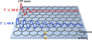 Charge transfer at material interfaces governs a wide range of physical properties, from electronic band structures to emergent collective excitations. In two-dimensional (2D) material heterostructures, charge transfer phenomena play important roles in enabling novel quantum phases, proximity effects, and tunable plasmonic responses. One representative charge transfer interface is formed between α-RuCl3, a van der Waals material with high electron affinity, and graphene. Significant charge transfer across this interface induces the formation of charge-transfer plasmon polaritons (CPPs), hybrid excitations between light and charge oscillations. However, previous studies found that as the charge transfer process takes place, α-RuCl3 becomes lossy, which limits the quality factor of CPPs. Here, we investigate CPPs down to 10 K using a home-built scattering-type scanning near-field optical microscope (s-SNOM) optimized for low-temperature measurements. Our study reveals a dramatic suppression of plasmon loss channels below 40 K, contributing to a significant enhancement in the plasmonic quality factor. This reduction in loss is likely attributed to the blue shift of the correlation-induced Mott gap in α-RuCl3 with decreasing temperature, along with the reduction of phonon scattering at low temperature. Our results highlight the potential of using s-SNOM and CPPs to study complex 2D interfaces and reveal correlated electron dynamics in the underlying material.
Electronic interactions in Dirac fluids visualized by nano-terahertz spacetime interference of electron-photon quasiparticles
Suheng Xu et al, Science Advances 10, eado5553 (2024) Ref. [365]
Details
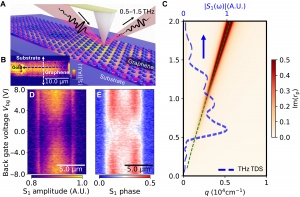 Ultraclean graphene at charge neutrality hosts a quantum critical Dirac fluid of interacting electrons and holes. Interactions profoundly affect the charge dynamics of graphene, which is encoded in the properties of its electron-photon collective modes: surface plasmon polaritons (SPPs). Here, we show that polaritonic interference patterns are particularly well suited to unveil the interactions in Dirac fluids by tracking polaritonic interference in time at temporal scales commensurate with the electronic scattering. Spacetime SPP interference patterns recorded in terahertz (THz) frequency range provided unobstructed readouts of the group velocity and lifetime of polariton that can be directly mapped onto the electronic spectral weight and the relaxation rate. Our data uncovered prominent departures of the electron dynamics from the predictions of the conventional Fermi-liquid theory. The deviations are particularly strong when the densities of electrons and holes are approximately equal. The proposed spacetime imaging methodology can be broadly applied to probe the electrodynamics of quantum materials.
Negative Refraction in Hyperbolic Heterobicrystals
Sternbach et al., Science 379, 555 (2023) Ref. [336]
Details
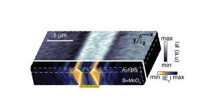 We visualized negative refraction of phonon polaritons, which occurs at the interface between two natural crystals. The polaritons—hybrids of infrared photons and lattice vibrations—form collimated rays that display negative refraction when passing through a planar interface between the two hyperbolic van der Waals materials: molybdenum oxide (MoO3) and isotopically pure hexagonal boron nitride (h11BN). At a special frequency ω0, these rays can circulate along closed diamond-shaped trajectories. We have shown that polariton eigenmodes display regions of both positive and negative dispersion interrupted by multiple gaps that result from polaritonic-level repulsion and strong coupling.
Infrared Plasmons Propagate Through a Hyperbolic Nodal Metal
Shao et al. Science Advances 8, 43 (2022) Ref. [331]
Details
 It is expected that layered anisotropic metals will support hyperbolic waveguiding. However, this behavior remains elusive, primarily because interband losses arrest the propagation of infrared modes. Here, we report on the observation of propagating hyperbolic waves in a prototypical layered nodal-line semimetal ZrSiSe. The observed waveguiding originates from polaritonic hybridization between near-infrared light and nodal-line plasmons. Unique nodal electronic structures simultaneously suppress interband loss and boost the plasmonic response, ultimately enabling the propagation of infrared modes through the bulk of the crystal.
Programmable Bloch polaritons in graphene
Xiong et al. Science Advances 7, eabe8087 (2021). Ref. [302]
Details
 We demonstrated efficient control of photons by hybridizing light with graphene Dirac electrons. Programmable control of photons is achieved by periodically modulating the carrier density of the Dirac electron using a proximate dielectric superlattice. In these periodic structures, common SPPs with continuous dispersion are transformed into Bloch polaritons with attendant discrete bands separated by bandgaps. We explored directional Bloch polaritons and steered their propagation by dialing the proper gate voltage. Fourier analysis of the near-field images corroborates that this novel on-demand nano-optics functionality is rooted in the polaritonic band structure. Our programmable polaritonic platform paves the way for the much-sought benefits of on-the-chip photonic circuits.
Charge-Transfer Plasmon Polaritons at Graphene/⍺-RuCl3 Interfaces
Rizzo et al. Nano Letters, 20, 8438 (2020) Ref [290]
Details
 Doped graphene is a robust platform for collective light-matter modes known as surface plasmon polaritons (SPPs). In our work, we demonstrate that the large work function of ⍺-RuCl3 can be exploited to create a massive charge density (>1013 cm-2) in graphene via charge-transfer across the 2D interface. Excitation of the resulting metallized graphene with light gives rise to three distinct types of charge-transfer plasmon polaritons (CPPs), which act as reporters of the nanoscale spatial dependence of interlayer charge transfer. The magnitude and minimum size of doping features in graphene generated in this manner surpasses what can be achieved with standard electrostatic gating, and are realized in a simplified, contactless device architecture.
Fizeau drag in graphene plasmonics
Dong, Xiong et al. Nature 594, 513 (2021) Ref. [305]
Details
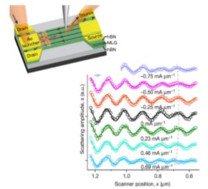 The current-induced Fizeau drag of graphene plasmons is visualized for the first time through infrared nano-imaging. The plasmon polaritons in graphene shorten their wavelength when propagating against the drifting carriers. Unlike the Fizeau effect for light, the plasmonic Fizeau drag by electrical currents defies explanation by simple kinematics and is linked to the nonlinear electrodynamics of Dirac electrons in graphene. The observed plasmonic drag enables breaking of time-reversal symmetry and reciprocity at infrared frequencies without resorting to magnetic fields or chiral optical pumping. The Fizeau drag also provides a tool with which to study interactions and nonequilibrium effects in electron liquids.
Polaritons in van der Waals materials
Basov, Fogler and Abajo Science 354, 195 (2016). Ref. [232]
Details
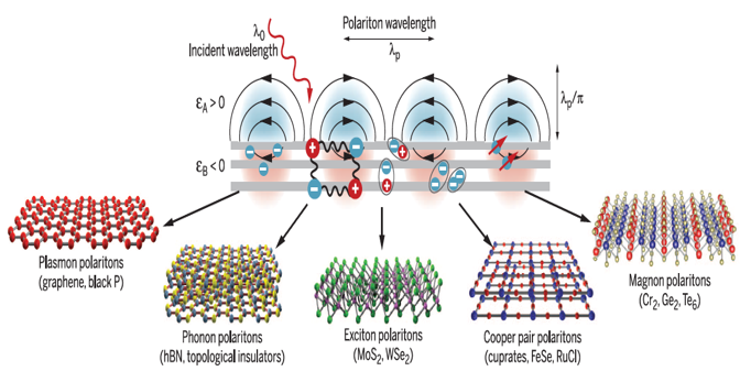 Interfaces of van der Waals materials sustain hybrid light-matter modes involving collective oscillations of polarization charges in matter, hence the term polaritons. Surface plasmon polaritons, supported by electrons in metals, constitute a most-studied prominent example. Yet there are many other varieties of polaritons, including those formed by atomic vibrations in polar insulators, excitons in semiconductors, Cooper pairs in superconductors, and spin resonances in (anti) ferromagnets. Together, they span a broad region of the electromagnetic spectrum, ranging from microwave to ultraviolet wavelengths.
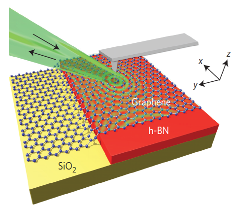
Nano-photocurrent Mapping of Local Electronic Structure in Twisted Bilayer Graphene
Sunku, McLeod et al. Nano Letters 20, 2958 (2020). Ref. [281]
Details
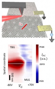 Twisted bilayer graphene (TBG) is known to contain spatial variations in the twist angle. In this work, we show that scanning nano-photocurrent imaging is a fast and non-invasive technique for determining the twist angle of TBG with nano-scale spatial resolution.
Photocurrent generation in graphene is dominated by the photothermoelectric effect. Incident light heats the carriers in graphene which then generate a thermoelectric voltage when they encounter a variation of the Seebeck coefficient.
One such variation is the boundary between twisted bilayer graphene and monolayer graphene. By scanning across the boundary while changing the carrier density, we were able to determine the local twist angle of TBG with nano-scale spatial resolution.
Photonic crystals for nano-light in moiré graphene superlattices
Sunku et al. Science 362, 1153 (2018). Ref. [263]
Details
Twisted bilayer graphene (TBG) consists of two graphene layers rotated relative to each other and forming a Moire pattern. At small twist angles, atomic reconstruction leads to the formation of periodic domain wall solitons that host topologically protected chiral states. Previous work [Jiang et al, Nano Lett, 17:7080 (2017)] has shown that plasmon polaritons in graphene are efficiently scattered by the domain wall solitons. We used infrared nano-imaging to study the properties of plasmons propagating in small twist angle TBG. We discovered that, the periodic soliton network transforms the TBG into a natural plasmon photonic crystal, where the origin of the plasmon scattering is a purely quantum effect. In addition, we showed that the properties of the TBG based photonic crystal are sensitive to the twist angle, providing a new control knob for tuning plasmons in graphene.
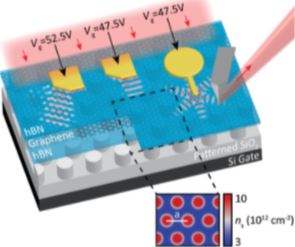
Fundamental limits to graphene plasmonics
Ni et al. Nature 557, 530 (2018). Ref. [257]
Details
Nano-IR imaging of graphene surface plasmons in layered Au/hBN/G/hBN/SiO2/Si heterostructure at cryogenic temperature. The entire field of view is within the diffraction-limited spot of our IR laser, which operates at an energy of 110 meV. Nano-IR image of plasmonic fringes from the encapsulated graphene monolayer, expressed by the normalized scattering amplitude s acquired at a back-gate voltage of 97 V and a temperature of T = 60 K. The arrows represent the propagation direction of the plasmon waves. These experiments simultaneously visualize the local electric field associated with interference from plasmon polaritons emitted by the near-field probe and reflected by sample edges, as well as from polaritons emitted by the Au microstructures.
Ultrafast optical switching of infrared plasmon polaritons in high-mobility graphene
Ni et al. Nature Photonics 10, 244 (2016). Ref. [225]
Details
 Graphene is emerging as one of the most capable candidates for plasmonic media for infrared wavelengths. Here we visualize and elucidate the properties of non-equilibrium photo-induced plasmons in a high-mobility graphene monolayer4.We activate plasmons with femtosecond optical pulses in a specimen of graphene that otherwise lacks infrared plasmonic response at equilibrium. In combination with static nano-imaging results on plasmon propagation, our infrared pump–probe nano-spectroscopy investigation reveals new aspects of carrier relaxation in heterostructures based on high-purity graphene.
Plasmons in graphene moiré superlattices
Ni et al. Nature Materials 14, 1217 (2015) Ref. [215]
Details
 Moiré patterns are superlattice structures that appear when two crystals with a minor lattice mismatch are superimposed. A prominent recent example is that of monolayer graphene placed on a crystal of hexagonal boron nitride. To probe the dynamical response of the moiré graphene, we use infrared (IR) nano-imaging to explore propagation of surface plasmons, collective oscillations of electrons coupled to IR light. We show that interband transitions associated with the superlattice mini-bands in concert with free electrons in the Dirac bands produce two additive contributions to composite IR plasmons in graphene moiré superstructures.
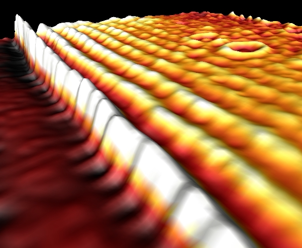
Tunable Phonon Polaritons in Atomically Thin van der Waals Crystals of Boron Nitride
Dai et al. Science 343, 1125 (2014). Ref. [187]
Details
 van der Waals heterostructures assembled from atomically thin crystalline layers of diverse two-dimensional solids are emerging as a new paradigm in the physics of materials. We used infrared nanoimaging to study the properties of surface phonon polaritons in a representative van der Waals crystal, hexagonal boron nitride. We launched, detected, and imaged the polaritonic waves in real space and altered their wavelength by varying the number of crystal layers in our specimens. The measured dispersion of polaritonic waves was shown to be governed by the crystal thickness according to a scaling law that persists down to a few atomic layers. Our results are likely to hold true in other polar van der Waals crystals and may lead to new unctionalities.