Facilities and Key Instruments
Our group at Columbia runs a state-of-the art laboratory for optical and nano-optical characterization of complex materials. The versatility of infrared and optical methods can be appreciated from a quick inspection of characteristic energy scales in solids which all fall in the frequency range that can be covered using a series of instruments available in our group. Development of novel spectroscopic instrumentation is an integral part of our research effort. Some examples can be seen below.
Infrared Nano-Spectroscopy and Nano-Imaging at Cryogenic Temperature

Terahertz Nano-Spectroscopy and Nano-Imaging at Cryogenic Temperature
Pump-Probe Nano-Spectroscopy and Nano-Imaging (Pharos – Neaspec)
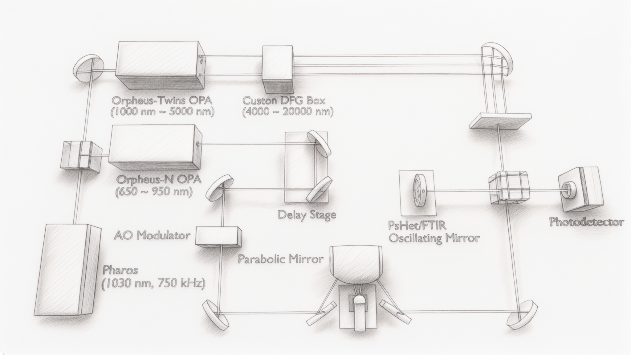
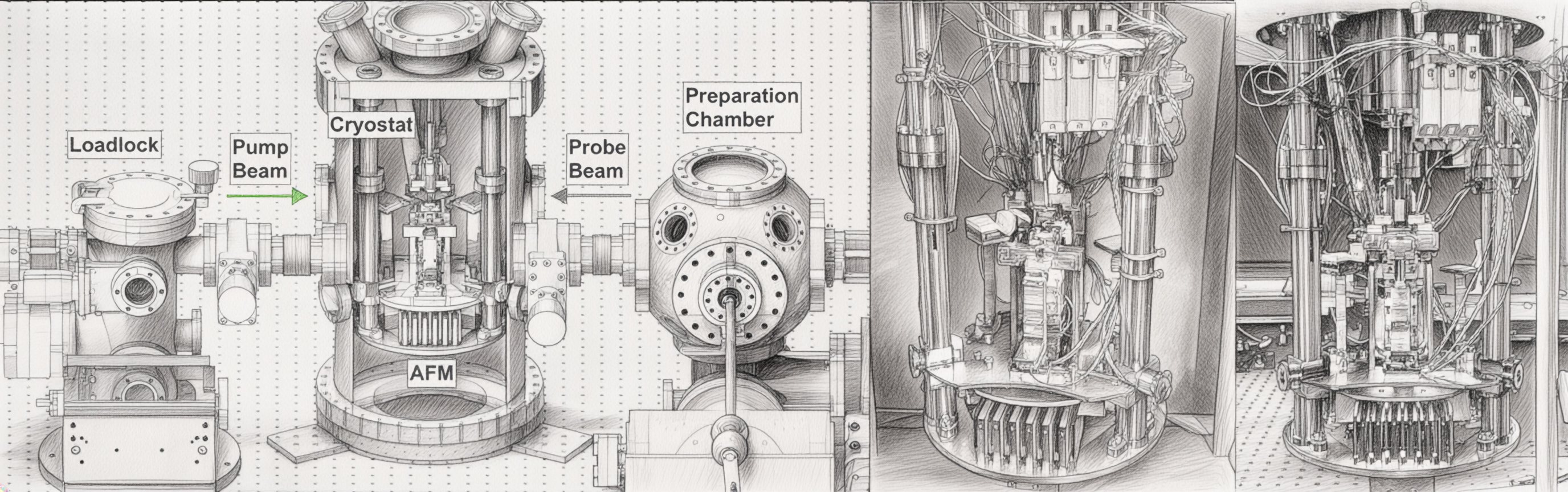
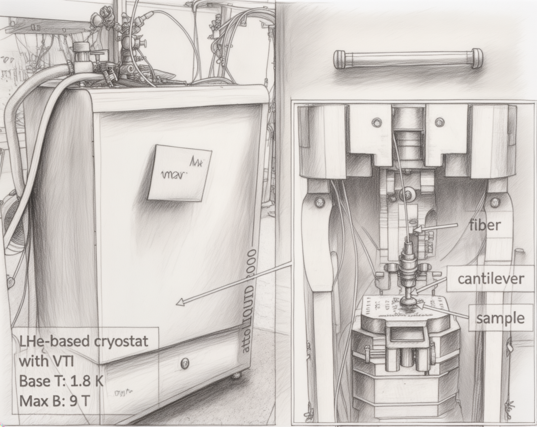
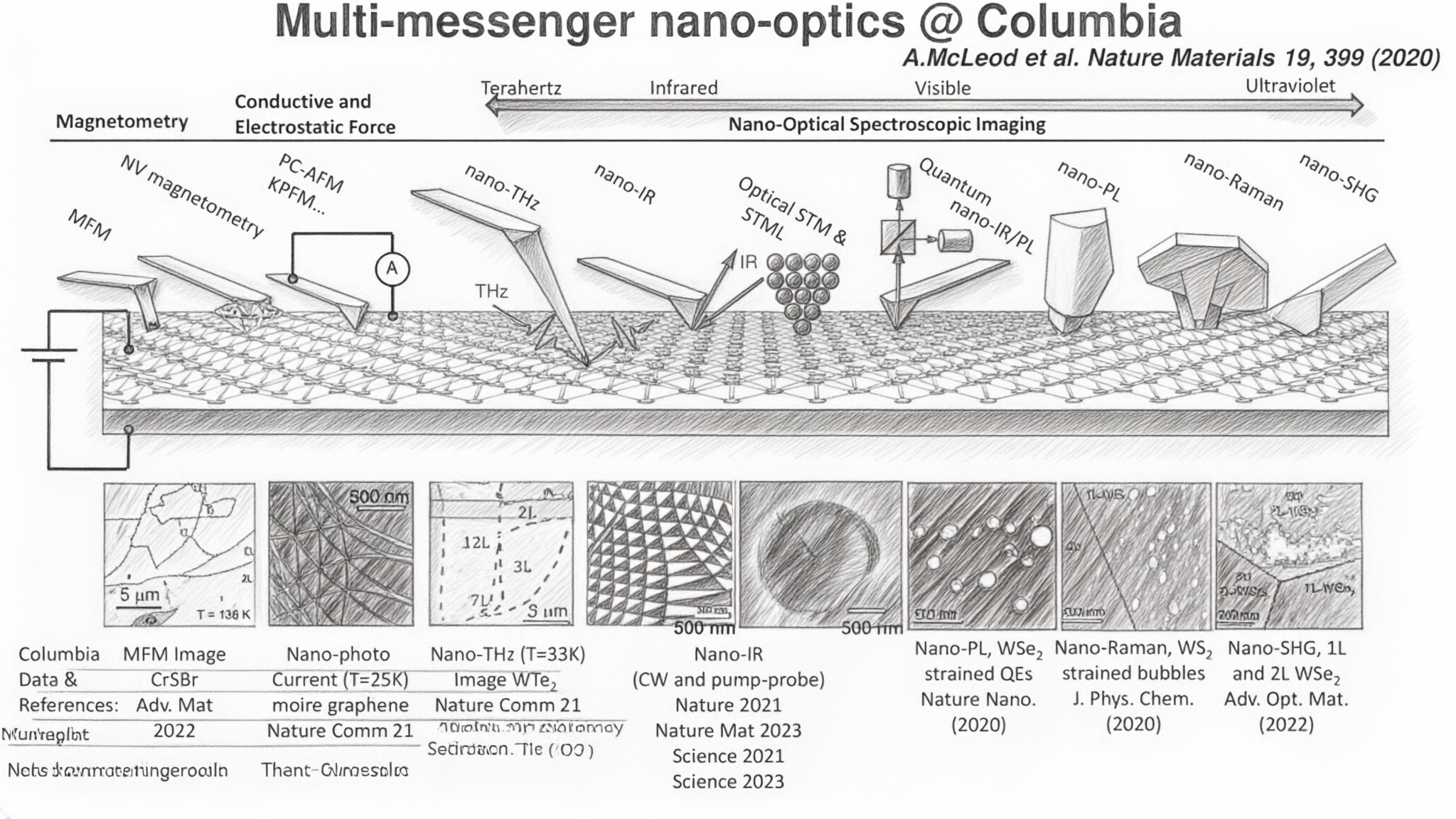
Table 1. Experimental characteristics of spectroscopic instruments available in the Basov laboratory at Columbia.

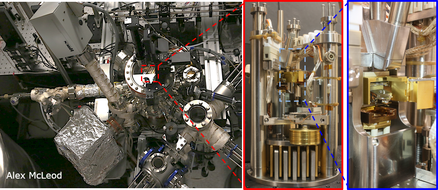 Our three home-built cryo-SNOMs has capability of nano-imaging down to resolution of 15nm and temperature of 18K with energy ranging from visible (600nm-1.2um) to MIR (3um-11um) and THz(1-2THz). The systems have extendable, multi-messenger functions such has nano-photocurrent mapping, KPFM and MFM as well.
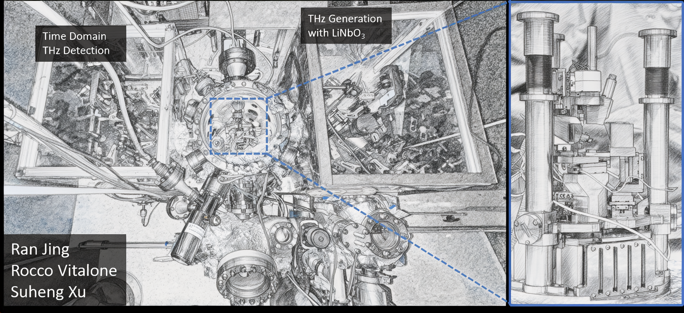
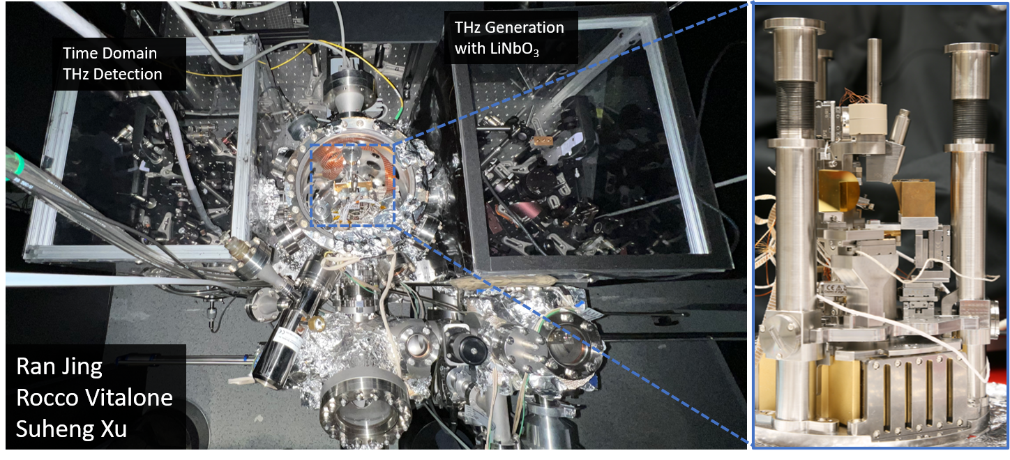 Our lab’s second custom-built cryogenic SNOM is dedicated to near-field imaging and spectroscopy within the terahertz (THz) frequency range (0.4-2.5 THz), offering nanometer spatial resolution, femtosecond temporal resolution, and temperature control down to 25 K. Using two different sources, a high-field THz source (LiNBO3) and low-field THz source (photo conductive antenna), the system supports THz near-field scattering, ultra-fast optical pump-THz probe, and ultra-fast optical pump-THz near-field emission. The nano-THz signal is detected in the time-domain through electro-optical sampling, which yields both amplitude and phase information of the scattered electric field. Combining femtosecond-scale time-domain detection with nano-scale spatial resolution, our system introduces an innovative experimental protocol to monitor propagating collective modes in spacetime. The sample exchange apparatus allows for high-throughput measurements and with in-situ electrical contacts to the sample for electrical gating, current drive, resistivity measurements, and magnetic fields. Articles [
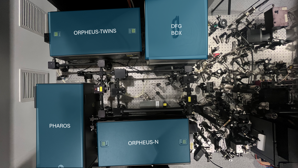
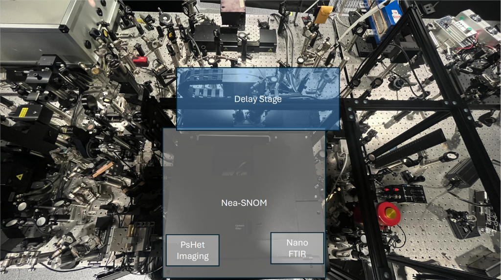 Combining intense ultrafast lasers with near-field microscopy creates novel opportunities for material exploration and discovery. Our beamline covers the spectral range of 660 -20,000 nm with a single light source. When used as a probe of a materials' properties, this broadband radiation can be tuned to selectively interrogate specific electronic, vibrational or rotational modes in materials of interest. The information is acquired with 10 nm spatial resolution independent of the wavelength of radiation used. Similarly, a second light channel from the same source can be tuned to control, or pump, specific modes in the materials. By using an acousto-optic modulator to "turn-off" every other pump pulse, and isolating information from both ON and OFF probe pulses with digital boxcars we are able to reference the near-field signal on a pulse-to-pulse basis. This extremely sensitive detection method is used to monitor the photo-excited and equilibrium states of materials with nanometer spatial resolution and femtosecond temporal resolution. The nano-meter scale confinement of probe radiation further implies that we probe a finite momentum, well outside what can be accessed by conventional optics. The ultrafast nano-IR beamline provides access to photo-excited states with momenta in-between what can be accessed by conventional optics and x-ray sources in a tabletop setting. These studies have been applied to Ultrafast plasmons in Graphene, as well as Plasmonic modes in InAs. Articles: [
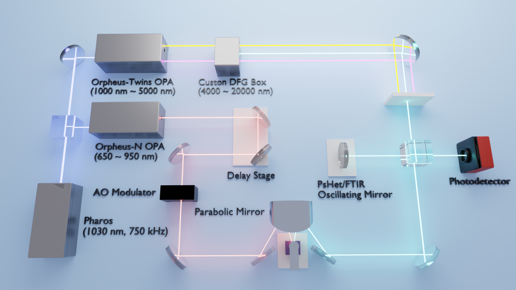
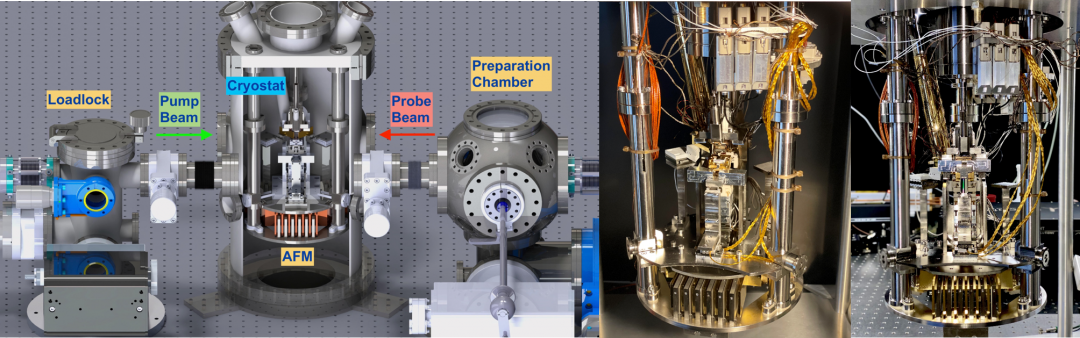 Cryosnom-3 is our third home-built cryogenic SNOM. Cryonom-3 vacuum pressure can reach down to ~ 10-11 torr and can work at 18 K-350 K. The beam lines and detectors covers the spectral range of 700 nm-116000 nm. At all these wavelengths, the spatial resolution of the scattering light measurement can reach down to 20 nm. Besides the optical measurement capability, side-band KPFM and MFM are also integrated into the system. In addition, there are 9 electrodes on the sample holder, allowing in-situ electrical transport and nano-photocurrent measurements. Check back in the future for links to papers published using Cryo-SNOM-III.
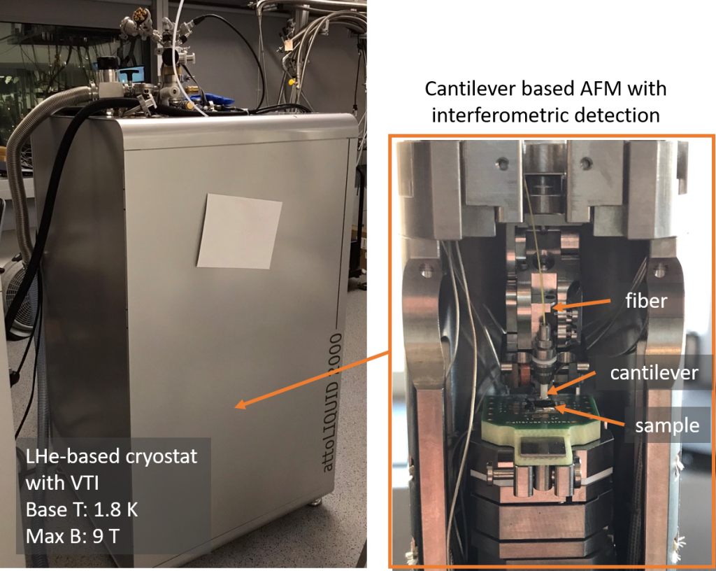 The Attocube cryogenic AFM/MFM is one of our newest instruments. It has a liquid helium-based cryostat with sample temperature variable from 1.8 K to room temperature and magnetic field up to 9T. This cantilever-based atomic force microscope (AFM) with interferometric detection is primarily used for magnetic force microscopy (MFM) to image magnetic domains in bulk, thin film, and device-based samples. With in-situ transport capabilities, this instrument is ideal for investigating magnetic and superconducting phases of materials and devices. Check back in the future for links to papers published using the Attocube cryogenic AFM/MFM.
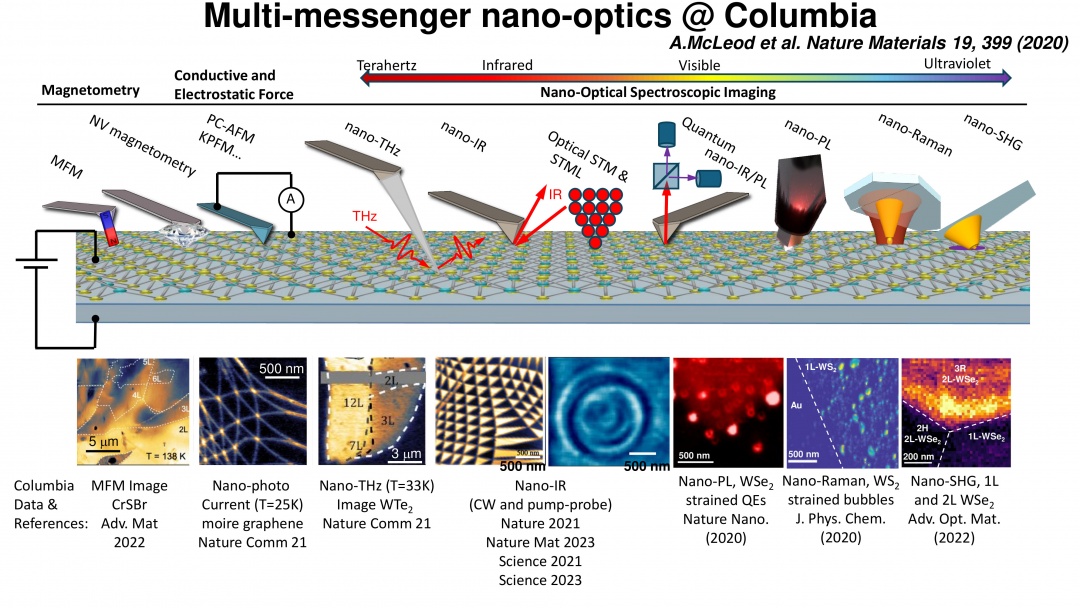 The broad family of scanning probe techniques accessible with a traditional cantilever-mounted atomic force microscope (AFM) permits simultaneous characterization of topographic (AFM), magnetic (MFM), electro-potential (KPFM), opto-electronic (nano-photocurrent), optical (SNOM, nano-THz, nano-PL), and non-linear optical (nano-SHG) behavior at the nanoscale. This form of multi-messenger nano-imaging provides unprecedented access to the rich interplay of spatially-correlated emergent properties in quantum materials. Articles [