Electromagnetic Metamaterials & Hyperbolic Media
Electromagnetic metamaterials are man-made materials comprised of structures whose electromagnetic properties are deliberately engineered to offer a range of response difficult or impossible to achieve in naturally occurring materials or composites. Some astounding applications of metamaterials include (but are not limited to); negative index of refraction (where magnetic and electric response are simultaneously negative), “perfect” (sub-wavelength) lensing, and electromagnetic “invisibility” cloaks. The Basov lab is focused at new implementations of metamaterials. In parallel, we investigate hyperbolic (meta)materials suitable for sub-diffractional imaging and focusing of infrared radiation.
Good plasmons in a bad metal
Ruta et al., Science 387, 786 (2025) Ref. [371]
Details
 Correlated metals may exhibit unusually high resistivity that increases linearly in temperature, breaking through the Mott-Ioffe-Regel bound, above which coherent quasiparticles are destroyed. The fate of collective charge excitations, or plasmons, in these systems is a subject of debate. Several studies have suggested that plasmons are overdamped, whereas other studies have detected propagating plasmons. In this work, we present direct nano-optical images of low-loss hyperbolic plasmon polaritons (HPPs) in the correlated van der Waals metal MoOCl2. HPPs are plasmon-photon modes that waveguide through extremely anisotropic media and are remarkably long-lived in MoOCl2. Photoemission data presented here reveal a highly anisotropic Fermi surface, reconstructed and made partly incoherent, likely through electronic interactions as explained by many-body theory. HPPs remain long-lived despite this, revealing previously unseen imprints of many-body effects on plasmonic collective modes.
Hyperbolic exciton polaritons in a van der Waals magnet
Ruta et al., Nature Communications, 14, 8261 (2023) Ref. [350]
Details
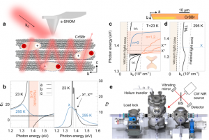 Exciton polaritons are quasiparticles of photons coupled strongly to bound electron-hole pairs, manifesting as an anti-crossing light dispersion near an exciton resonance. Highly anisotropic semiconductors with opposite-signed permittivities along different crystal axes are predicted to host exotic modes inside the anti-crossing called hyperbolic exciton polaritons (HEPs), which confine light subdiffractionally with enhanced density of states. Here, we show observational evidence of steady-state HEPs in the van der Waals magnet chromium sulfide bromide (CrSBr) using a cryogenic near-infrared near-field microscope. At low temperatures, in the magnetically-ordered state, anisotropic exciton resonances sharpen, driving the permittivity negative along one crystal axis and enabling HEP propagation. We characterize HEP momentum and losses in CrSBr, also demonstrating coupling to excitonic sidebands and enhancement by magnetic order: which boosts exciton spectral weight via wavefunction delocalization. Our findings open new pathways to nanoscale manipulation of excitons and light, including routes to magnetic, nonlocal, and quantum polaritonics.
Negative Refraction in Hyperbolic Heterobicrystals
Sternbach et al., Science 379, 555 (2023) Ref. [336]
Details
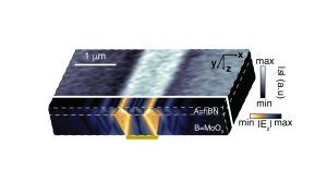 We visualized negative refraction of phonon polaritons, which occurs at the interface between two natural crystals. The polaritons—hybrids of infrared photons and lattice vibrations—form collimated rays that display negative refraction when passing through a planar interface between the two hyperbolic van der Waals materials: molybdenum oxide (MoO3) and isotopically pure hexagonal boron nitride (h11BN). At a special frequency ω0, these rays can circulate along closed diamond-shaped trajectories. We have shown that polariton eigenmodes display regions of both positive and negative dispersion interrupted by multiple gaps that result from polaritonic-level repulsion and strong coupling.
Infrared Plasmons Propagate Through a Hyperbolic Nodal Metal
Shao et al. Science Advances 8, 43 (2022) Ref. [331]
Details
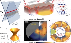 It is expected that layered anisotropic metals will support hyperbolic waveguiding. However, this behavior remains elusive, primarily because interband losses arrest the propagation of infrared modes. Here, we report on the observation of propagating hyperbolic waves in a prototypical layered nodal-line semimetal ZrSiSe. The observed waveguiding originates from polaritonic hybridization between near-infrared light and nodal-line plasmons. Unique nodal electronic structures simultaneously suppress interband loss and boost the plasmonic response, ultimately enabling the propagation of infrared modes through the bulk of the crystal.
Programmable Hyperbolic Polaritons in Van der Waals Semiconductors
Sternbach et al. Science 371, 6529 (2021) Ref. [293]
Details
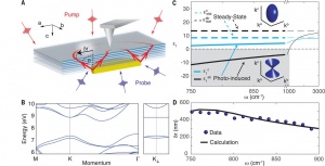 Collective electronic modes or lattice vibrations usually prohibit propagation of electromagnetic radiation through the bulk of common materials over a frequency range associated with these oscillations. Though in layered crystals highly anisotropic materials often display nonintuitive optical properties and can permit propagation of subdiffractional waveguide modes, with hyperbolic dispersion, throughout their bulk. Here, we report on the observation of optically induced electronic hyperbolicity in the layered transition metal dichalcogenide tungsten diselenide (WSe2). By using photoexcitation to inject electron-hole pairs in WSe2 , we were able to visualize the hyperbolic rays that traveled along conical trajectories inside of the crystal, thus establishing here the signatures of programmable hyperbolic electrodynamics and assessing the role of quantum transitions of excitons within the Rydberg series in the observed polaritonic response.
Graphene on hexagonal boron nitride as a tunable hyperbolic metamaterial
Dai et al. Nature Nanotechnology 10, 682 (2015). Ref. [209]
Details
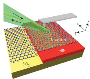 Hexagonal boron nitride (h-BN) is a natural hyperbolic material. Owing to this property, finite-thickness slabs of h-BN act as multimode waveguides for the propagation of hyperbolic phonon polaritons. Here we show, by direct nano-infrared imaging, that these hyperbolic polaritons can be effectively modulated in a van der Waals heterostructure composed of monolayer graphene on h-BN. The hyperbolic plasmon–phonon polaritons possess the combined virtues of surface plasmon polaritons in graphene and hyperbolic phonon polaritons in h-BN. Therefore, graphene/h-BN can be classified as an electromagnetic metamaterial as the resulting properties of these devices are not present in its constituent elements alone.
Subdiffractional focusing and guiding of polaritonic rays in a natural hyperbolic material
Dai et al. Nature Communications 6, 6963 (2015). Ref. [205]
Details
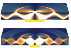 In hyperbolic materials, light propagation is unusual leading to novel and often non-intuitive optical phenomena. Here we report infrared nano-imaging experiments demonstrating that crystals of hexagonal boron nitride, a natural mid-infrared hyperbolic material, can act as a ‘hyper-focusing lens’ and as a multi-mode waveguide. The lensing is manifested by subdiffractional focusing of phonon–polaritons launched by metallic disks underneath the hexagonal boron nitride crystal. Our work opens new opportunities for anisotropic layered insulators in infrared nanophotonics complementing and potentially surpassing concurrent artificial hyperbolic materials with lower losses and higher optical localization.
Voltage switching of a VO2 memory metasurface using ionic gel
Goldflam et al. Applied Physics Letters 105, 041117 (2014) . Ref. [195]
Details
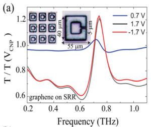 We demonstrate an electrolyte-based voltage tunable vanadium dioxide (VO2 ) memory metasurface. Large spatial scale, low voltage, non-volatile switching of terahertz (THz) metasurface resonances is achieved through voltage application using an ionic gel to drive the insulator-to-metal transition in an underlying VO2 layer. Positive and negative voltage application can selectively tune the metasurface resonance into the “off” or “on” state by pushing the VO2 into a more conductive or insulating regime respectively. Compared to graphene based control devices, the relatively long saturation time of resonance modification in VO2 based devices suggests that this voltageinduced switching originates primarily from electrochemical effects related to oxygen migration across the electrolyte–VO2 interface.

