Cavity Quantum Materials
Is it feasible to alter the ground state properties of a material by engineering its electromagnetic environment? Inspired by theoretical predictions, experimental realizations of such cavity-controlled properties without optical excitation are beginning to emerge. Our group devised and implemented a novel platform to realize cavity-altered materials based on van der Walls crystals and heterostructures. We exploit a suite of scanning nano-probe techniques to inquire into the physics of cavity-matterials interactions.
Highlights:
Cavity-Altered Superconductivity
Itai Keren et al. Nature 650, 864–868 (2026). Ref. [398].
Details
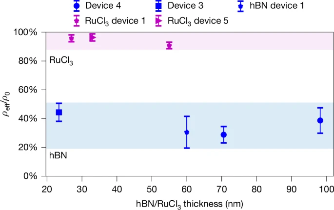 Is it feasible to alter the ground-state properties of a material by engineering its electromagnetic environment? Inspired by theoretical predictions, experimental realizations of such cavity-controlled properties without optical excitation are beginning to emerge. Here we devised and implemented a new platform to realize cavity-altered materials. Single crystals of hyperbolic van der Waals (vdW) compounds provide a resonant electromagnetic environment with enhanced density of photonic states and prominent mode confinement. We interfaced hexagonal boron nitride (hBN) with the molecular superconductor κ-(BEDT-TTF)2Cu[N(CN)2]Br (κ-ET). The frequencies of infrared hyperbolic modes (HMs) of hBN match the infrared-active carbon–carbon (C=C) stretching molecular resonance of κ-ET implicated in superconductivity. Nano-optical data supported by first-principles molecular Langevin dynamics simulations confirm the presence of resonant coupling between the hBN hyperbolic cavity modes and the C=C stretching mode in κ-ET. Meissner-effect measurements using magnetic force microscopy (MFM) demonstrate a strong suppression of superfluid density near the hBN/κ-ET interface. Non-resonant control heterostructures, including RuCl3/κ-ET and hBN/Bi2Sr2CaCu2O8+x(BSCCO), do not show the pronounced superfluid suppression. These observations suggest that hBN/κ-ET realizes a cavity-altered superconducting ground state. Our work highlights the potential of dark cavities devoid of external photons for engineering electronic ground-state properties of complex quantum materials.
Molecular Plasmonic Cavities
Daniel J. Rizzo et al., Nano Letters 25, 14043–14050 (2025). Ref. [386].
Details
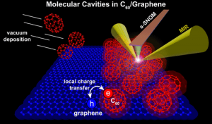 Graphene-based photonic structures have emerged as fertile ground for the controlled manipulation of surface plasmon polaritons (SPPs), providing a two-dimensional platform with low optoelectronic losses. In principle, nanostructuring graphene can enable further confinement of nanolight─enhancing light-matter interactions in the form of SPP cavity modes. In this study, we engineer nanoscale plasmonic cavities composed of self-assembled C60 arrays on graphene. Using scattering-type scanning near-field optical microscopy (s-SNOM) in conjunction with first-principles density functional theory (DFT) calculations, we show that C60 assemblies behave as molecular plasmonic cavities, giving rise to precisely defined hole-doped regions within continuous samples of graphene. By tuning the deposition conditions of C60, the lateral dimensions of molecular cavities can be tailored to the SPP wavelength. Finite-element simulations verify the existence of SPP cavity modes, revealing a real-space pattern characteristic of confined SPPs. Thus, our study provides a straightforward scheme for tailoring SPP mode volume by leveraging molecular self-assembly.
Van der Waals waveguide quantum electrodynamics probed by infrared nano-photoluminescence
Samuel L. Moore et al., Science Advances 11, eadh5672 (2025). Ref. [382].
Details
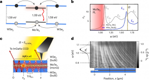 Atomically layered van der Waals (vdW) materials exhibit remarkable properties, including highly confined infrared waveguide modes and the capacity for infrared emission in the monolayer limit. Here we engineered structures that leverage both of these nano-optical functionalities. Specifically, we encased a photoluminescing atomic sheet of MoTe2 within two bulk crystals of WSe2, forming a vdW waveguide for the embedded light-emitting monolayer. The modified electromagnetic environment offered by the WSe2 waveguide alters MoTe2 spontaneous emission—a phenomenon we directly image with our interferometric nano-photoluminescence technique. We captured spatially oscillating nanoscale patterns prompted by spontaneous emission from MoTe2 into waveguide modes of WSe2 slabs. We quantify the resulting Purcell-enhanced emission rate within the framework of a waveguide quantum electrodynamics model, relating the MoTe2 spontaneous emission rate to the measured waveguide dispersion. Our work marks a substantial advance in the implementation of all-vdW quantum electrodynamics waveguides.